Silicon-based heterojunction solar cell structure and preparation method thereof

A solar cell and heterojunction technology, applied in circuits, photovoltaic power generation, electrical components, etc., can solve problems such as impracticality, complicated process, and theoretical parameters, and achieve good gettering effect, reduced recombination, and reduced impact effects

Pending Publication Date: 2022-02-25
SUZHOU AIKANG LOW CARBON TECH INST +1
View PDF7 Cites 0 Cited by
  • Summary
  • Abstract
  • Description
  • Claims
  • Application Information

AI Technical Summary

Problems solved by technology

In the prior art, there is no cell structure to further improve the photoelectric efficiency of heterojunction solar cells from the perspective of single crystal silicon substrates, the process is complex, and the parameters achieved are theoretical, which is not practical

Method used


Image

  • Silicon-based heterojunction solar cell structure and preparation method thereof

Examples


Embodiment 1

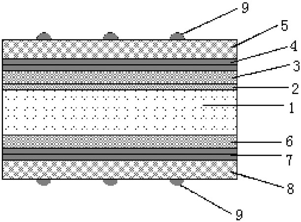
[0023] see figure 1 , a kind of silicon-based heterojunction solar cell structure that the present invention relates to, it comprises N-type monocrystalline silicon substrate 1, and the front side of described N-type monocrystalline silicon substrate 1 is provided with a layer of n+ doped layer 2, in n+ A first intrinsic amorphous silicon / microcrystalline silicon film 3 is deposited on the surface of the doped layer 2, and no less than two layers of n-type silicon are deposited on the surface of the first intrinsic amorphous silicon / microcrystalline silicon film 3. Amorphous silicon / microcrystalline silicon film 4, a layer of first conductive film 5 is deposited on the surface of the outermost n-type amorphous silicon / microcrystalline silicon film 4;

[0024] The back side of the N-type monocrystalline silicon substrate 1 is provided with a layer of second intrinsic amorphous silicon / microcrystalline silicon film 6, and the surface of the second intrinsic amorphous silicon / mic...


PUM


Abstract

The invention relates to a silicon-based heterojunction solar cell structure and a preparation method thereof, the silicon-based heterojunction solar cell structure comprises an N-type monocrystalline silicon substrate, the front surface of the N-type monocrystalline silicon substrate is provided with an n + doping layer, a first intrinsic amorphous silicon/microcrystalline silicon film is deposited on the surface of the n + doping layer, no less than two layers of n-type amorphous silicon/microcrystalline silicon films are deposited on the surface of the first intrinsic amorphous silicon/microcrystalline silicon film, and a layer of first conductive film is deposited on the surface of the outermost layer of n-type amorphous silicon/microcrystalline silicon film; and a layer of second intrinsic amorphous silicon/microcrystalline silicon film is arranged on the back surface of the N-type monocrystalline silicon substrate, no less than two layers of p-type amorphous silicon/microcrystalline silicon films are deposited on the surface of the second intrinsic amorphous silicon/microcrystalline silicon film, and a layer of second conductive film is deposited on the surface of the outermost layer of p-type amorphous silicon/microcrystalline silicon film. The n + doping layer is formed on the main surface of the N-type monocrystalline silicon substrate to form a high-low junction, so that a certain separation effect on photon-generated carriers is achieved, and recombination of the photon-generated carriers is reduced.

Description

technical field [0001] The invention relates to the technical field of photovoltaic high-efficiency cells, in particular to a silicon-based heterojunction solar cell structure and a preparation method thereof. Background technique [0002] Silicon-based heterojunction solar cells are recognized by the photovoltaic industry as the next generation of photovoltaic cell technology that can be mass-produced due to their high photoelectric conversion efficiency. The silicon-based heterojunction solar cell structure includes n-type single crystal silicon substrate, amorphous silicon / crystalline silicon film, transparent conductive film, metal electrode and so on. The conventional preparation steps include: preparation and cleaning of suede surface, deposition of amorphous silicon / microcrystalline silicon film, deposition of transparent conductive film, and preparation of metal electrodes by electroplating or screen printing. Conventional process thinking, such as Chinese patent CN...

Claims


Application Information

Patent Timeline
Patent Type & Authority Applications(China)
IPC IPC(8): H01L31/0352H01L31/0747H01L31/18H01L31/20
CPCH01L31/035272H01L31/0747H01L31/202H01L31/186Y02E10/50Y02P70/50
Inventor 连维飞
Owner SUZHOU AIKANG LOW CARBON TECH INST
Why Eureka
Try Eureka