Process method for assembling PCB substrate antenna and carrier structural member

An assembly process and structural part technology, which is applied in the manufacture of antenna array devices, antennas, antenna arrays, etc., can solve the problems of difficult production, low assembly yield, and high assembly difficulty, and achieve the improvement of radiation efficiency and operating frequency. , Improve the electrical performance index, the effect of good welding effect

Active Publication Date: 2022-02-25
10TH RES INST OF CETC
View PDF8 Cites 0 Cited by
  • Summary
  • Abstract
  • Description
  • Claims
  • Application Information

AI Technical Summary

Problems solved by technology

The second type is to use different layers of antenna arrays to achieve different polarizations respectively. The disadvantage is that the structure is complex, the production is difficult, and the cost is high.
However, the welding process of the high-density microstrip antenna and the metal carrier plate is very difficult to assemble and has always been a problem. The penetration rate is less than 50%, the RF through-hole is short-circuited, and the assembly yield is extremely low. There are almost no successful cases.
[0010] 2. The poor penetration rate of the PCB substrate antenna and the carrier structure will cause an air section between the printed board and the metal base. The impact on the performance of the antenna is mainly reflected in the increase of the voltage standing wave ratio, resulting in a phased array antenna. The radiation efficiency decreases
If the area of ​​the air section is large, it may even cause a serious shift in the operating frequency of the antenna. Therefore, the penetration rate is the key to determining the electrical performance index. It is a huge challenge for the welding of large-scale, high-density, and small-pitch array antennas.
Due to the above problems, the performance of the antenna index is very satisfactory, which limits the development of the millimeter-wave phased array antenna to the extremely miniaturized side. In order to reduce the impact of the above problems, it is urgent to solve the technical problems of large-scale high-density welding technology and improve Process integration capability

Method used


Image

  • Process method for assembling PCB substrate antenna and carrier structural member
  • Process method for assembling PCB substrate antenna and carrier structural member
  • Process method for assembling PCB substrate antenna and carrier structural member

Examples


Embodiment Construction

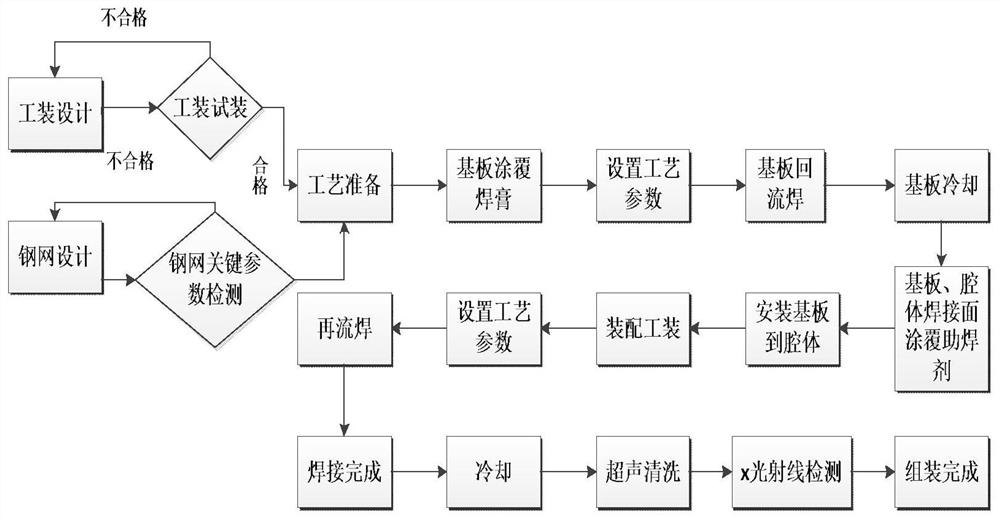
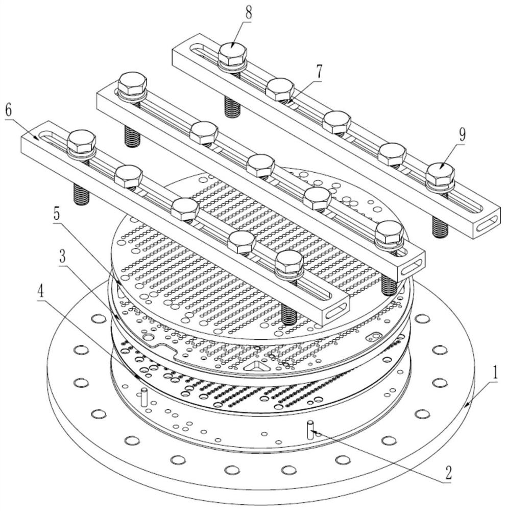
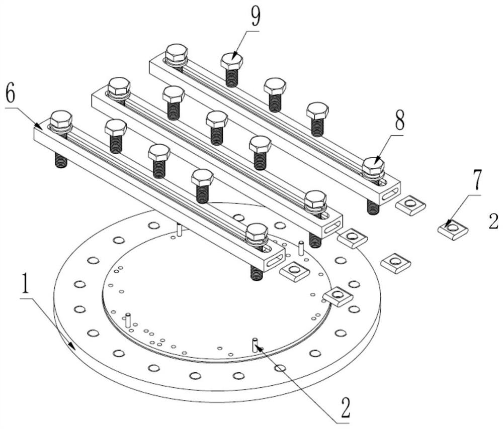
[0027] refer to figure 1 , figure 2 . According to the present invention, for the antenna array module composed of the carrier structure 3, the KA frequency band PCB substrate antenna 4, the fur button assembly, the metal cover plate, etc., a solder coating tool for matching the external dimensions of the PCB substrate antenna 4 is prepared And welding tooling, apply solder paste on the welding area at the bottom of PCB substrate antenna 4 through solder coating tooling, because the welding density is too high, first use solder coating tooling to apply solder to the soldering surface of PCB substrate antenna 4, and then place it on the heating plate for reflow Solder paste on the PCB substrate antenna 4, cool the PCB substrate antenna 4, and complete the solder fixation on the PCB substrate antenna 4; apply flux to the welding surface of the PCB substrate antenna 4 and carrier structure 3 that has been coated with solder, and install the PCB substrate Antenna 4 to carrier ...


PUM


Abstract

The invention discloses a process method for assembling a micro-strip array antenna PCB substrate antenna 4 and a carrier structural member, and aims to provide a process method capable of improving the welding yield of a PCB substrate antenna and a carrier and reducing the voidage. According to the technical scheme, the method comprises the steps that a solder coating tool and a welding tool which are matched with a printed circuit board (PCB) substrate antenna in shape are prepared, solder is applied to the welding face of the PCB substrate antenna through the solder coating tool, reflowing solder paste on a heating plate is placed after the solder is controlled, the PCB substrate antenna is cooled, and solder fixing is completed; the printed board PCB substrate antenna and the carrier structural member are fixed through a welding tool; and the PCB substrate antenna and the carrier structural member which are provided with the tool are put into a reflow soldering furnace together, and the PCB substrate antenna and the carrier structural member are finally fixed together through reflow soldering, thereby completing the welding assembly of the PCB substrate antenna and the carrier structural member.

Description

technical field [0001] The invention relates to an assembly process method suitable for 512 array elements of KA frequency band dual-polarized microstrip array printed board PCB substrate antenna 4 and carrier structural member 3, especially for applications with broadband dual-polarization high isolation and high polarity The dual-polarization microstrip array printed board PCB substrate antenna 4 antenna and the carrier structural member 3 assembly process method for the requirements of chemical purity. Background technique [0002] Active phased array (AESA) radar has become the standard configuration of modern advanced fighters. Its target tracking / searching capability, high resolution, strong electronic interference and high data communication capabilities far surpass radars with traditional mechanical scanning systems. . [0003] With the development of microelectronics and micromechanical technology, AESA has also penetrated into the missile-borne radar seeker field ...

Claims


Application Information

Patent Timeline
Patent Type & Authority Applications(China)
IPC IPC(8): H01Q21/00
CPCH01Q21/0087
Inventor 李颖凡陈中良王文川王彪金珂谢义水
Owner 10TH RES INST OF CETC
Why Eureka
Try Eureka