Supercharge Your Innovation With Domain-Expert AI Agents!

Organic compound, electronic element and electronic device

A technology of organic compounds and chemical formulas, applied in electrical components, organic chemistry, organic chemical methods, etc., can solve problems affecting the service life of materials, damage to film uniformity, and low glass transition temperature, so as to improve aggregation and hole migration rate, the effect of high hole mobility

Active Publication Date: 2022-03-04
SHAANXI LIGHTE OPTOELECTRONICS MATERIAL CO LTD
View PDF6 Cites 5 Cited by
  • Summary
  • Abstract
  • Description
  • Claims
  • Application Information

AI Technical Summary

Problems solved by technology

Due to the generally small molecular weight of the currently reported hole transport layer materials, the glass transition temperature of the material is low; during the use of the material, repeated charge and discharge will make the material easy to crystallize and the uniformity of the film will be destroyed, thus affecting the service life of the material

Method used


Image

  • Organic compound, electronic element and electronic device
  • Organic compound, electronic element and electronic device
  • Organic compound, electronic element and electronic device

Examples


Embodiment 1

[0137] Embodiment 1: red organic electroluminescent device

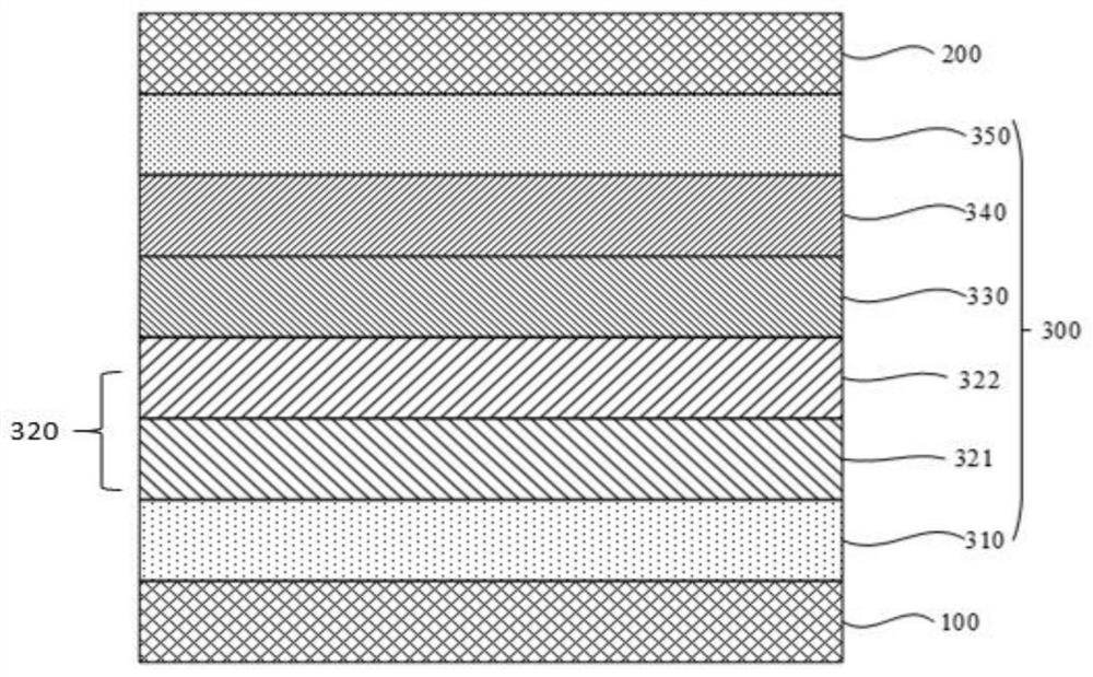
[0138] The anode was prepared by the following process: the thickness was The ITO / Ag / ITO substrate (manufactured by Corning) was cut into a size of 40mm × 40mm × 0.7mm, and it was prepared into an experimental substrate with cathode, anode and insulating layer patterns by using a photolithography process, using ultraviolet ozone and O 2 :N 2 Plasma was used for surface treatment to increase the work function of the anode (experimental substrate) and to remove scum.

[0139] Vacuum evaporation on the experimental substrate (anode) The HAT-CN is used as the hole injection layer (HIL), and then evaporated on the hole injection layer NPB, forming the first hole transport layer (HTL).

[0140] Compound 13 is vacuum evaporated on the first hole transport layer to form the second hole transport layer.

[0141] On the second hole-transporting layer, combine RH-1 with Ir(piq) 2 (acac) is co-evaporated at a 95%:5% e...

Embodiment 2~55

[0145] An organic electroluminescent device was fabricated using the same method as in Example 1, except that compounds shown in Table 8 below were used instead of Compound 13 when forming the second hole transport layer.


PUM


Abstract

The invention relates to an organic compound, an electronic element and an electronic device. The structural formula of the organic compound is shown as a chemical formula I. The organic compound is applied to an organic electroluminescent device, and the performance of the device can be remarkably improved.

Description

technical field [0001] The present application belongs to the technical field of organic materials, and in particular relates to an organic compound, an electronic component and an electronic device. Background technique [0002] With the development of electronic technology and the progress of material science, the application range of electronic components for realizing electroluminescence or photoelectric conversion is becoming wider and wider. Such electronic components generally include a cathode and an anode oppositely arranged, and a functional layer arranged between the cathode and the anode. The functional layer is composed of multiple organic or inorganic film layers, and generally includes an energy conversion layer, a hole transport layer located between the energy conversion layer and the anode, and an electron transport layer located between the energy conversion layer and the cathode. [0003] Taking an organic electroluminescent device as an example, it gene...

Claims


Application Information

Patent Timeline
Patent Type & Authority Applications(China)
IPC IPC(8): C07C211/56C07C255/58C07C211/58C07F7/10C07D307/91C07D409/12C07D333/76C07C211/61C07D209/86C07D405/12C07D209/88H01L51/50H01L51/54
CPCC07C211/56C07C255/58C07C211/58C07F7/081C07D307/91C07D409/12C07D333/76C07C211/61C07D209/86C07D405/12C07D209/88C07B2200/05C07C2603/26C07C2603/18C07C2603/42C07C2603/94H10K85/615H10K85/622H10K85/624H10K85/626H10K85/631H10K85/636H10K85/633H10K85/6574H10K85/6576H10K85/40H10K85/6572H10K50/15Y02E10/549H10K50/156C09K11/06H10K50/00C07C2603/97C07C211/54C09K2211/1011C09K2211/1014C09K2211/1018
Inventor 贾志艳张鹤鸣李应文金荣国
Owner SHAANXI LIGHTE OPTOELECTRONICS MATERIAL CO LTD
Features
  • R&D
  • Intellectual Property
  • Life Sciences
  • Materials
  • Tech Scout
  • Unparalleled Data Quality
  • Higher Quality Content
  • 60% Fewer Hallucinations
Learn More