
Patsnap Eureka
For R&D, Patsnap Eureka makes reading and utilizing patents & technical documents easy.
Patsnap Eureka AIR
Designed for self-driven R&D workflows. Generate viable solutions, solve complex R&D challenges, empower your innovation with AI.

Patsnap Eureka Materials
Designed for material experts only. Revolutionize your material R&D, from search, analyze, to developing new materials.

TechResearch
Generate reliable direction feasibility study reports for your R&D in just a few steps.

TechSeek
Discover and master advanced knowledge NOW. Basics, ideas, possibilities, all at once.

TechMind
As an expert in R&D Theories, TechMind can generates customized viable solutions instantly.

TechRisk
Analyze your overall solution with one click, know your potential R&D risks in advance.

TechMonitor
Get weekly tech updates, stay abreast of the latest tech innovations and key insights.
Method for improving heat dissipation performance of blue and green light semiconductor laser
A technology of heat dissipation performance and semiconductor, applied in the direction of semiconductor lasers, lasers, laser parts, etc., can solve the problems such as the problem of heat dissipation of the substrate cannot be effectively solved, the volume power density of related microwave power devices is increased, etc., and the yield is high. , low cost, and the effect of improving thermal conductivity
- Summary
- Abstract
- Description
- Claims
- Application Information
AI Technical Summary
Problems solved by technology
Method used
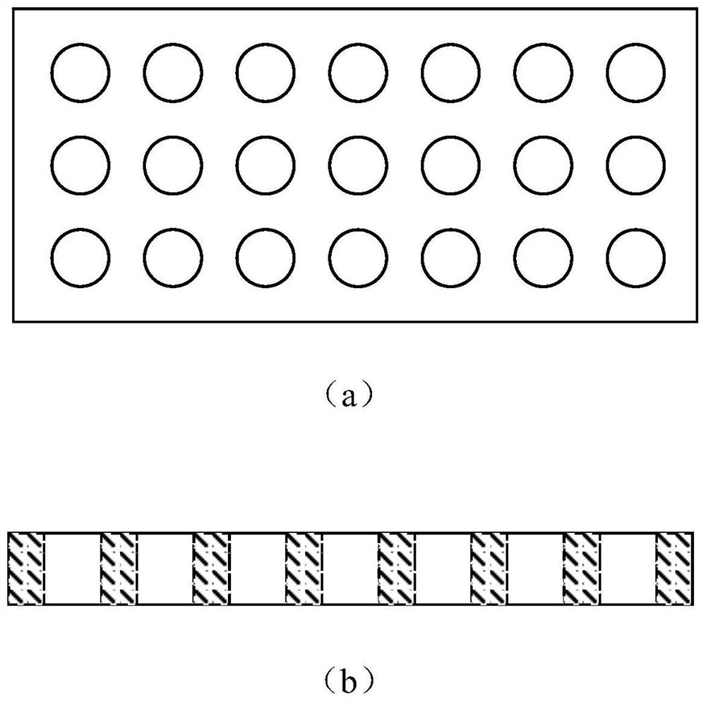
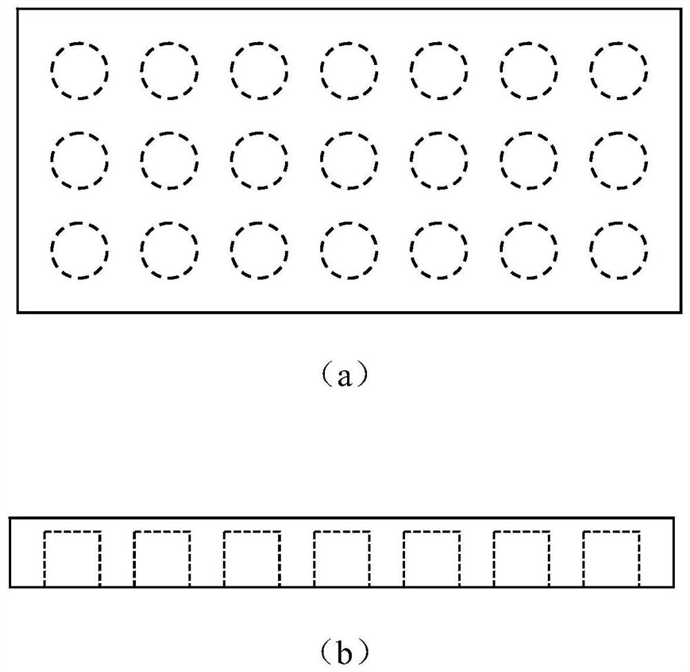
Image

Examples
Embodiment 1
[0034]This embodiment provides a blue and green laser whose substrate is filled with diamond material, including undoped GaN or n-GaN layered on a diamond-filled GaN or SiC (n-Type) substrate sequentially from bottom to top. Growth epitaxial layer, n-AlGaN or n-AlGaN / n-GaN superlattice lower confinement layer, undoped InGaN or n-InGaN lower waveguide layer or n-InGaN / n-GaN lower double waveguide layer, low temperature undoped GaN or undoped InGaN insertion layer, InGaN / GaN or InGaN / InGaN quantum well structure, undoped GaN or undoped InGaN upper protection layer, undoped InGaN upper waveguide layer or undoped InGaN / GaN upper double waveguide layer, p-AlGaN or p-AlGaN / p-GaN superlattice electron blocking layer, p-AlGaN or p-AlGaN / p-GaN superlattice upper confinement layer, polarization-induced p-AlGaN or p-NiO epitaxial layer , p++-GaN or p-InGaN ohmic contact layer.
[0035] The blue and green lasers whose substrate is filled with diamond materials are prepared through the fo...
Embodiment 2
[0054] This embodiment provides a blue and green laser whose substrate is filled with diamond material, including undoped GaN or n-GaN layered on a diamond-filled GaN or SiC (n-Type) substrate sequentially from bottom to top. Growth epitaxial layer, n-AlGaN or n-AlGaN / n-GaN superlattice lower confinement layer, undoped InGaN or n-InGaN lower waveguide layer or n-InGaN / n-GaN lower double waveguide layer, low temperature undoped GaN or undoped InGaN insertion layer, InGaN / GaN or InGaN / InGaN quantum well structure, undoped GaN or undoped InGaN upper protection layer, undoped InGaN upper waveguide layer or undoped InGaN / GaN upper double waveguide layer, p-AlGaN or p-AlGaN / p-GaN superlattice electron blocking layer, p-AlGaN or p-AlGaN / p-GaN superlattice upper confinement layer, polarization-induced p-AlGaN or p-NiO epitaxial layer , p++-GaN or p-InGaN ohmic contact layer.
[0055] The blue and green lasers whose substrate is filled with diamond materials are prepared through the f...
PUM
| Property | Measurement | Unit |
|---|---|---|
| thickness | aaaaa | aaaaa |
| thickness | aaaaa | aaaaa |
| thickness | aaaaa | aaaaa |
Abstract
Description
Claims
Application Information
 - R&D Engineer
- R&D Manager
- IP Professional
- Industry Leading Data Capabilities
- Powerful AI technology
- Patent DNA Extraction
Browse by: Latest US Patents, China's latest patents, Technical Efficacy Thesaurus, Application Domain, Technology Topic, Popular Technical Reports.
© 2024 PatSnap. All rights reserved.Legal|Privacy policy|Modern Slavery Act Transparency Statement|Sitemap|About US| Contact US: help@patsnap.com