Rear-end integrated structure of memristor unit and CMOS (complementary metal oxide semiconductor) circuit and preparation method of rear-end integrated structure

A memristor and circuit technology, applied in the field of microelectronic device technology and integrated circuits, to achieve the effect of realizing electrical connection, saving quantity, and saving process steps

Pending Publication Date: 2022-03-18
HUAZHONG UNIV OF SCI & TECH
View PDF0 Cites 0 Cited by
  • Summary
  • Abstract
  • Description
  • Claims
  • Application Information

AI Technical Summary

Problems solved by technology

[0006] Aiming at the above defects or improvement needs of the prior art, the present invention provides a back-end integrated structure of a memristor unit and a CMOS circuit and a preparation method thereof, so as to solve the problem that the prior art cannot realize the memristor under the condition of guaranteeing the performance of the memristor. Technical issues of electrical connection of memristor cells to CMOS circuits

Method used


Image

  • Rear-end integrated structure of memristor unit and CMOS (complementary metal oxide semiconductor) circuit and preparation method of rear-end integrated structure
  • Rear-end integrated structure of memristor unit and CMOS (complementary metal oxide semiconductor) circuit and preparation method of rear-end integrated structure
  • Rear-end integrated structure of memristor unit and CMOS (complementary metal oxide semiconductor) circuit and preparation method of rear-end integrated structure

Examples


Embodiment 1

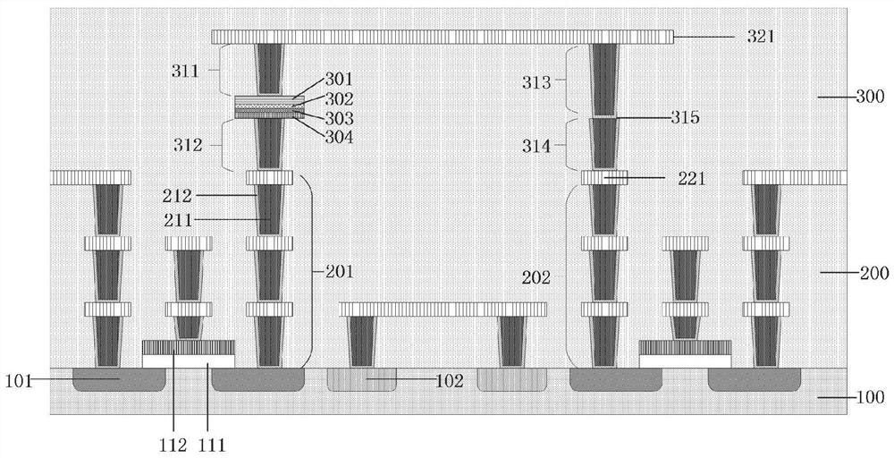
[0056] A back-end integrated structure of a memristor unit and a CMOS circuit, such as figure 1 As shown, including: MOSFET structure, metal interconnection layer and memristor layer distributed sequentially from bottom to top;

[0057] The MOSFET structure includes a substrate 100 and a first transistor and a second transistor prepared on the substrate 100; wherein, the first transistor and the second transistor are transistors in a CMOS circuit; in some optional implementation manners, the MOSFET structure is in the form of Based on the single crystal silicon substrate, including transistors and other electronic components based on CMOS front-end technology, together constitute a basic planar bulk silicon MOSFET structure; wherein, the transistor includes source / drain doped regions 101, substrate heavily doped Region 102, gate oxide layer 111, polysilicon gate 112 and so on. It should be noted that the MOSFET structure may also be other MOSFET structures such as an advanced...

Embodiment 2

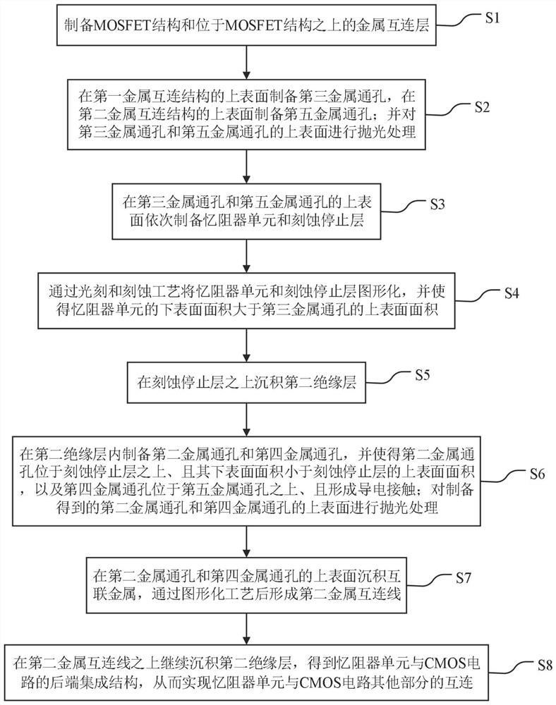
[0070] A method for preparing a back-end integrated structure of a memristor unit and a CMOS circuit, such as figure 2 shown, including the following steps:

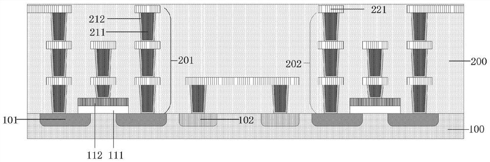
[0071] S1. Prepare a MOSFET structure and a metal interconnection layer located on the MOSFET structure; wherein, the MOSFET structure includes a substrate and a first transistor and a second transistor prepared on the substrate; the first transistor and the second transistor are in a CMOS circuit The transistor; the metal interconnection layer includes a first insulating layer, and a first metal interconnection structure and a second metal interconnection structure located inside the first insulating layer;

[0072]Wherein, the metal interconnection layer includes a first insulating layer, and a first metal interconnection structure and a second metal interconnection structure located inside the first insulating layer; in some optional implementation manners, the number of layers of the above metal interconnection stru...


PUM

PropertyMeasurementUnit
thicknessaaaaaaaaaa
thicknessaaaaaaaaaa

Abstract

The invention discloses a rear-end integrated structure of a memristor unit and a CMOS (complementary metal oxide semiconductor) circuit and a preparation method of the rear-end integrated structure, the memristor unit is arranged between two layers of metal interconnection lines and is communicated with upper and lower metal interconnection lines through metal through holes, and an etching stop layer is arranged on the memristor unit; the memristor structure can be effectively protected when the upper through hole of the memristor unit is etched, so that the memristor structure is not damaged while good butt joint of the metal through hole butt joint structure part can be achieved, and electrical connection between the memristor unit and a CMOS circuit can be achieved under the condition that the performance of the memristor is guaranteed. On the basis of a standard CMOS (Complementary Metal-Oxide-Semiconductor Transistor) process, a rear-end process integration method is adopted, so that hybrid integration of the memristor and a CMOS circuit is realized. According to the method provided by the invention, the memristor with high performance can be prepared on the metal interconnection layer on the basis of adding a small number of steps of processes and two layers of layouts, the interconnection between the memristor and a CMOS (Complementary Metal Oxide Semiconductor) circuit is realized, and the performance of the CMOS device is not influenced.

Description

technical field [0001] The invention belongs to the field of microelectronic device technology and integrated circuit technology, and more specifically relates to a back-end integrated structure of a memristor unit and a CMOS circuit and a preparation method thereof. Background technique [0002] With the advent of the Internet of Things and the era of big data, the amount of data generated by human society is increasing geometrically, which puts forward higher requirements for information processing, transmission and storage. However, as the size of CMOS devices shrinks to 3-5nm process nodes, the size reduction driven by Moore's Law is about to fail, the Von Neumann bottleneck caused by the separation of storage and calculation in traditional computers, and the storage wall caused by the speed gap between Flash and DRAM And other problems seriously limit the development of information technology. Therefore, the key to breakthroughs is the development of new Beyond CMOS de...

Claims


Application Information

Patent Timeline
Patent Type & Authority Applications(China)
IPC IPC(8): H01L27/24H01L21/768H01L23/48H01L23/50H01L45/00
CPCH01L23/50H01L23/481H01L21/76898H01L21/76895H10B63/30H10N70/801
Inventor 王兴晟王成旭阳帆黄梦华缪向水
Owner HUAZHONG UNIV OF SCI & TECH
Why Eureka
Try Eureka