Chip processing equipment capable of fully etching wafer

A technology for processing equipment and chips, applied in the manufacture of conveyor objects, electrical components, semiconductor/solid-state devices, etc., can solve the problems of insufficient wafer etching, easy corrosion of hand skin, poor etching effect, etc. Strong etching effect, sufficient etching and cleaning, preventing the effect of hand skin

Pending Publication Date: 2022-03-25
智多多(沈阳)科技有限公司
View PDF0 Cites 0 Cited by
  • Summary
  • Abstract
  • Description
  • Claims
  • Application Information

AI Technical Summary

Problems solved by technology

[0004] During etching, the staff manually pick and place the wafer in the fixture, which is time-consuming and laborious, and it is easy to corrode the skin of the hands. Moreover, since the wafer is fixed on the fixture according to a certain distance, the wafer will be damaged. There is a certain contact with the fixture, and a part of the wafer surface will be blocked, resulting in insufficient wafer etching and poor etching effect

Method used


Image

  • Chip processing equipment capable of fully etching wafer
  • Chip processing equipment capable of fully etching wafer
  • Chip processing equipment capable of fully etching wafer

Examples


Embodiment Construction

[0041] The technical solution of this patent will be further described in detail below in conjunction with specific embodiments.

[0042] Embodiments of the present invention are described in detail below, examples of which are shown in the drawings, wherein the same or similar reference numerals designate the same or similar elements or elements having the same or similar functions throughout. The embodiments described below by referring to the figures are exemplary only for explaining the present invention and should not be construed as limiting the present invention.

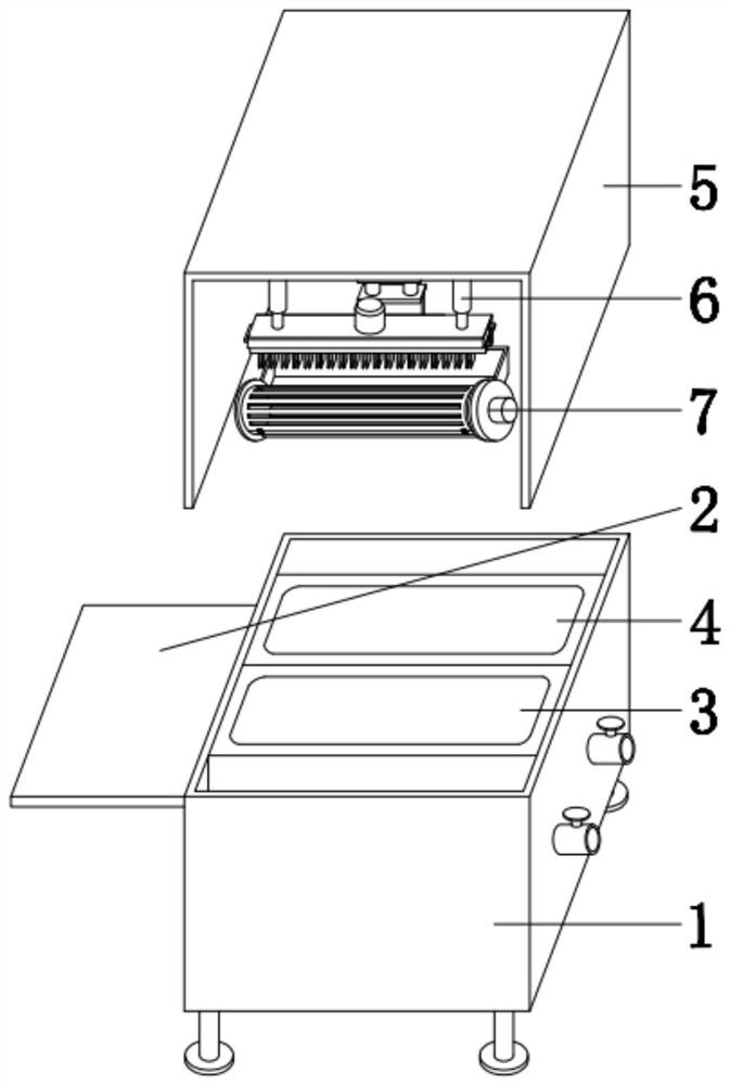
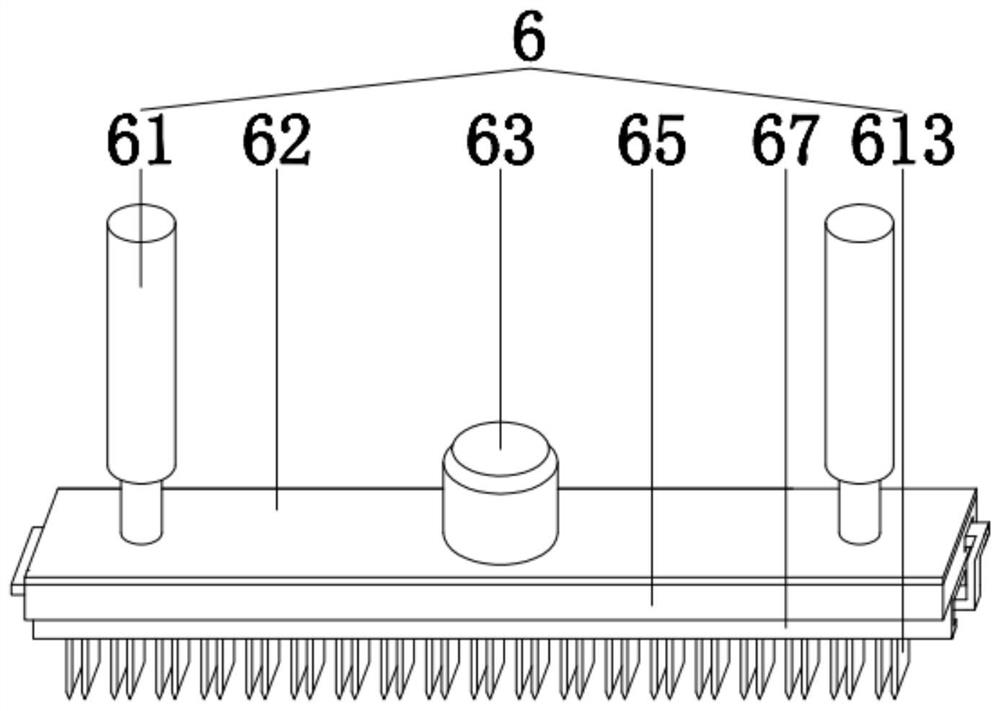
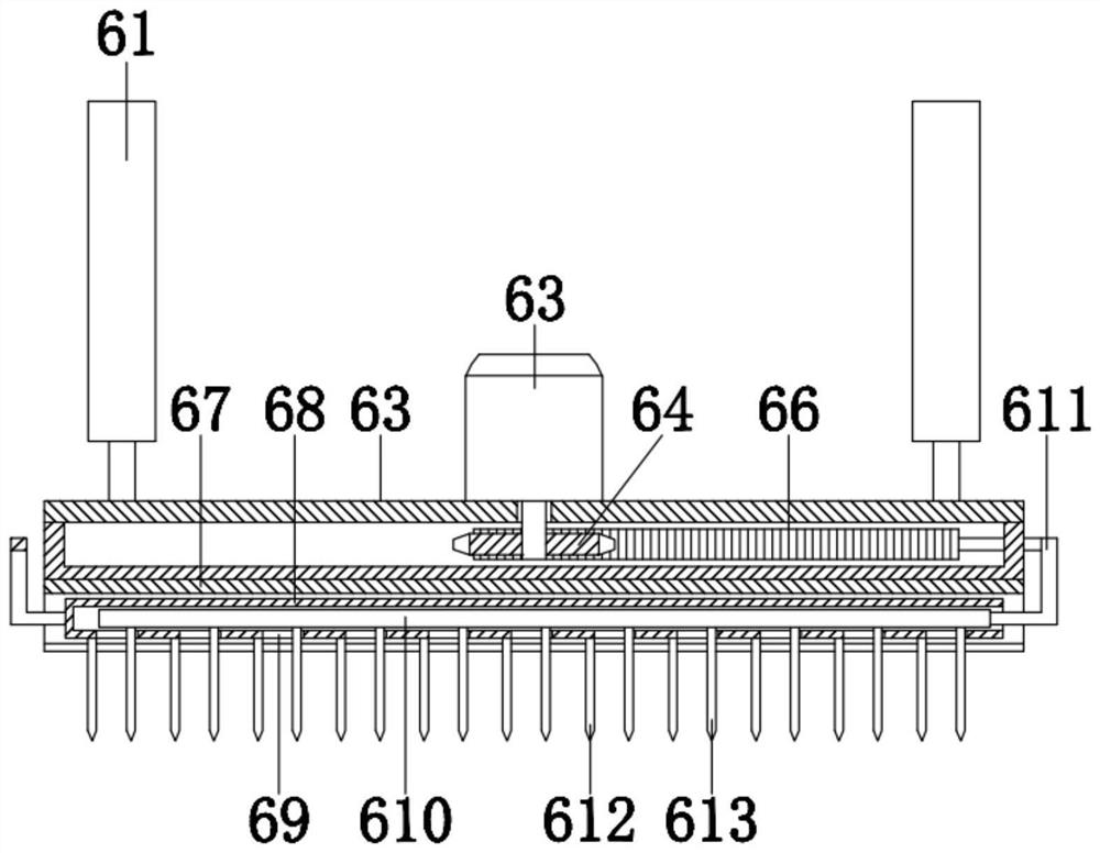
[0043] see Figure 1-4 , in an embodiment of the present invention, a chip processing equipment with sufficient wafer etching, including a box body 1, a supporting plate 2, a cleaning tank 3 and an etching tank 4, the supporting plate 2 is fixedly connected to the left side wall of the box body 1 The top is used to place the bracket with the wafer, the cleaning tank 3 is installed on the front side of the in...


PUM


Abstract

The invention relates to the field of chips, in particular to chip processing equipment sufficient in wafer etching, which comprises a box body, a supporting plate, a cleaning tank and an etching tank, the supporting plate is fixedly connected to the top end of the left side wall of the box body, the cleaning tank is mounted on the front side of an inner cavity of the box body, the etching tank is mounted on the rear side of the inner cavity of the box body, and the chip processing equipment further comprises a dustproof shell, the box body is fixedly connected to the top end of the box body; the feeding and discharging mechanism is mounted on the front side of the top end of the inner cavity of the dustproof shell; the diving mechanism is mounted at the top end of the inner cavity of the dustproof shell; the feeding and discharging mechanism comprises two first air cylinders which are installed on the left side and the right side of the top end of an inner cavity of the dustproof shell correspondingly. The top plate is mounted at the output end of the first air cylinder; and the first motor is mounted in the center of the top end of the top plate. According to the invention, automatic feeding and discharging of the wafer are realized, time and labor are saved, hand skin of a worker is prevented from being corroded, in addition, the purpose of fully etching and cleaning the wafer is achieved, the etching effect is strong, and the etching effectiveness is ensured.

Description

technical field [0001] The invention relates to the technical field of chips, in particular to chip processing equipment with sufficient wafer etching. Background technique [0002] Wafer refers to the silicon wafer used to make silicon semiconductor circuits, and its raw material is silicon. The production process includes steps such as single crystal pulling, slicing, grinding, polishing, layering, etching, and heat treatment; [0003] Etching includes dry method and wet method. The wet method mainly uses chemical etching, which is to soak the wafer in the silicon dioxide etching solution in the etching tank, etch with the assistance of ultrasonic waves, and then wash it with the cleaning solution in the cleaning tank to achieve removal. The purpose of wafer surface layer, especially suitable for wafer etching larger than 3μm; [0004] During etching, the staff manually pick and place the wafer in the fixture, which is time-consuming and laborious, and it is easy to corr...

Claims


Application Information

Patent Timeline
IPC IPC(8): H01L21/67H01L21/677H01L21/687
CPCH01L21/67086H01L21/67742H01L21/68721
Inventor 谢冰齐艳香
Owner 智多多(沈阳)科技有限公司
Why Eureka
Try Eureka