Method for improving electrical performance of InAlN/GaN high electron mobility transistor
A technology with high electron mobility and electrical performance, applied in the field of microelectronics research, can solve problems such as increasing the lattice mismatch between InAlN and GaN, reducing the mobility of two-dimensional electron gas, and breaking the lattice of the barrier layer. Effects of two-dimensional electron gas mobility, reduction of Coulomb field scattering, and reduction of on-resistance
- Summary
- Abstract
- Description
- Claims
- Application Information
AI Technical Summary
Problems solved by technology
Method used
Image
Examples
Embodiment 1
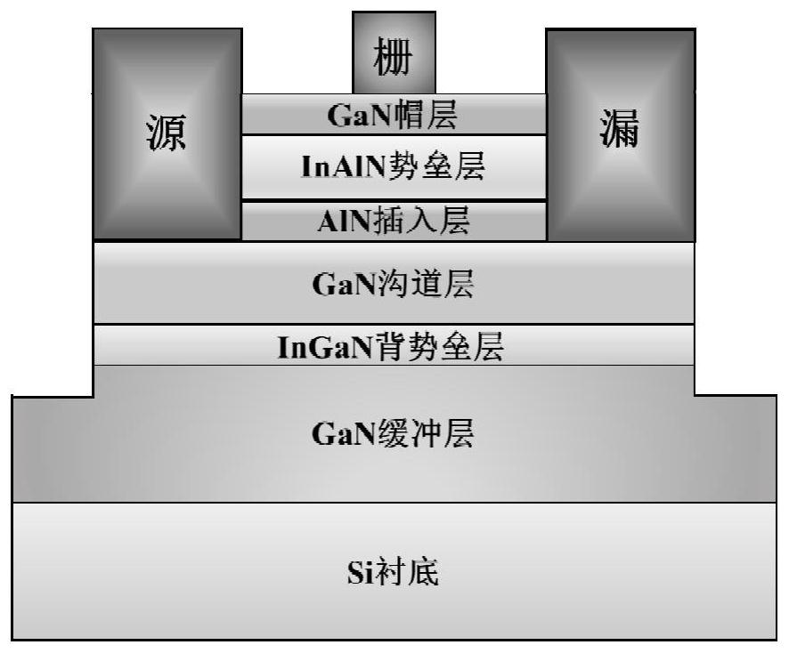
[0037] A method to improve the electrical performance of InAlN / GaN high electron mobility transistors, such as figure 1 As shown, the InAlN / GaN high electron mobility transistor includes a substrate, and the substrate is a Si substrate;
[0038] A GaN buffer layer located above the substrate, the thickness of the GaN buffer layer is 2-4 μm, and the GaN buffer layer is not doped;
[0039] An InGaN back barrier layer located above the GaN buffer layer, the thickness of the InGaN back barrier layer is 2-4nm, and the molar ratio of In is 10-15%;
[0040] A GaN channel layer located above the InGaN back barrier layer, the thickness of the GaN channel layer is 10-30nm;
[0041] An AlN insertion layer located above the GaN channel layer, the thickness of the AlN insertion layer is 0.7-1.5nm;
[0042] An InAlN barrier layer located above the AlN insertion layer, the thickness of the InAlN barrier layer is 5-9nm, and the molar ratio of In is 16-18%;
[0043] A GaN cap layer located ...
Embodiment 2
[0072] A method for improving the electrical performance of an InAlN / GaN high electron mobility transistor differs from the method for improving the electrical performance of an InAlN / GaN high electron mobility transistor provided in Example 1 in that:
[0073] In the prepared InAlN / GaN high electron mobility transistor, the thickness of the GaN buffer layer is 2 μm.
[0074] The thickness of the InGaN back barrier layer is 4 nm, and the molar ratio of In is 12%.
[0075] The GaN channel layer has a thickness of 15 nm.
[0076] The thickness of the AlN insertion layer is 1 nm.
[0077] The thickness of the InAlN barrier layer was 8 nm, and the molar ratio of In was 17%.
[0078] The thickness of the GaN cap layer is 2nm.
[0079] The distance between source and drain L SD is 15 μm.
[0080] Gate length L G , the distance between the gate and the source L GS , the distance between the gate and the drain L GD Both are 5 μm.
Embodiment 3
[0082] A method for improving the electrical performance of an InAlN / GaN high electron mobility transistor differs from the method for improving the electrical performance of an InAlN / GaN high electron mobility transistor provided in Example 1 in that:
[0083] The specific steps include: take 4mL of diluted 0.25mg / mL TFSI solution in the crystallization dish in the air environment, immerse the InAlN / GaN HEMT in the TFSI solution in the crystallization dish and place it in the air environment for 30s, take it out with N 2 Blow dry to complete the organic superacid treatment on the surface of InAlN / GaN HEMT.
PUM
| Property | Measurement | Unit |
|---|---|---|
| Thickness | aaaaa | aaaaa |
| Thickness | aaaaa | aaaaa |
| Thickness | aaaaa | aaaaa |
Abstract
Description
Claims
Application Information
 - Generate Ideas
- Intellectual Property
- Life Sciences
- Materials
- Tech Scout
- Unparalleled Data Quality
- Higher Quality Content
- 60% Fewer Hallucinations
Browse by: Latest US Patents, China's latest patents, Technical Efficacy Thesaurus, Application Domain, Technology Topic, Popular Technical Reports.
© 2025 PatSnap. All rights reserved.Legal|Privacy policy|Modern Slavery Act Transparency Statement|Sitemap|About US| Contact US: help@patsnap.com


