Edge-emitting type laser element

A laser component and side-firing technology, which is applied to laser components, lasers, electrical components, etc., can solve problems such as temperature rise, overflow, and active layer coupling efficiency reduction, so as to reduce the critical current value and improve the mode The effect of low gain and critical current value

Pending Publication Date: 2022-04-15
兆劲科技股份有限公司
View PDF0 Cites 0 Cited by
  • Summary
  • Abstract
  • Description
  • Claims
  • Application Information

AI Technical Summary

Problems solved by technology

In the structure of the aforementioned traditional FP laser element and DFB laser element, since the electrons from the n-type cladding layer and the lower optical confinement layer on the lower side of the laser element move faster than the p-type cladding layer on the upper side of the laser element And the holes in the optical confinement layer, so most of the electrons and holes will actually couple in the upper half of the active layer to emit light, which leads to the fact that the lower half of the active layer cannot be effectively used
In addition, this will also cause most of the light field to be biased in the upper half of the active layer (also known as the optical field offset in the vertical direction), and the coupling between the light field and the quantum well of the active layer is only biased in the upper half of the active layer. half, which also leads to the inability to increase the modal gain so that the critical current value cannot be reduced, nor can it reach a high operating rate (such as 10Gb / s) and cannot operate at high temperature
In summary, a larger critical current value means that more carrier density needs to be provided to cause population inversion to form laser and cause temperature rise, and carrier injection into the active layer will be easier as the temperature rises The phenomenon of overflow occurs, which also leads to a decrease in the coupling efficiency of carriers to the active layer

Method used


Image

  • Edge-emitting type laser element
  • Edge-emitting type laser element
  • Edge-emitting type laser element

Examples


Embodiment 1

[0042]

[0043] *Note: The thickness of the active layer can be designed according to the luminous wavelength range of the operating EEL element.

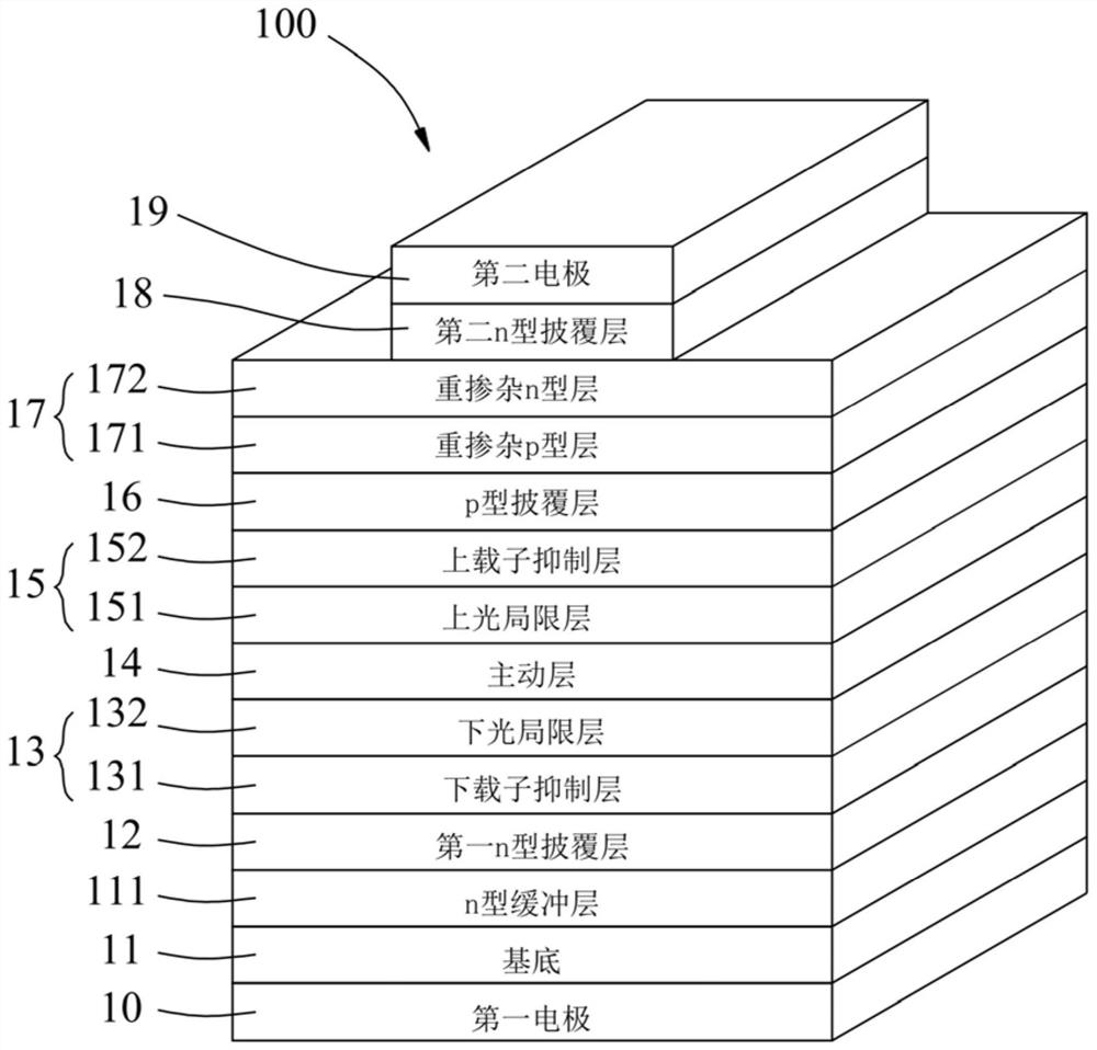
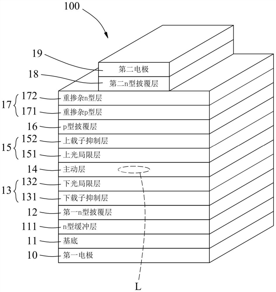
[0044] Corresponding to Comparative Example 1, Embodiment 1 produces the following advantages: (1) at the 11th layer, since Embodiment 1 adopts the tunnel junction layer 17 to combine the p-type cladding layer (12th layer) of Comparative Example 1 ) is transposed into the second n-type cladding layer 18 (the 12th layer) of embodiment 1, which makes embodiment 1 only have p-type cladding layer 16 (thickness 50nm) and the heavily doped p Type layer 171 (15nm) is a p-type semiconductor, and its total thickness is 65nm (65nm=50nm+15nm), but comparative example 1 has p-type cladding layer (50nm), etching stop layer (25nm), p-type cladding layer Layer (1500nm) and second electrode (200nm) are p-type semiconductors, and its total thickness is 1775nm (1775nm=50nm+25nm+1500nm+200nm), and the p-type semiconductor total thickness 65nm of e...

Embodiment 2

[0053]

[0054]

[0055] *Note: The thickness of the active layer can be designed according to the luminous wavelength range of the operating EEL element.

[0056] Similar to the discussion of Comparative Example 1 of the aforementioned FP laser element Table 1 and Example 1 of Table 2, corresponding to Comparative Example 2 of the DFB laser element, Example 2 also produces the following advantages: (1) on the 11th layer, Since Example 2 uses the tunnel junction layer 17 to transpose the p-type cladding layer (12th layer) of Comparative Example 2 into the second n-type cladding layer 18 (12th layer) of Example 2, this makes the implementation In Example 2, only the p-type cladding layer 16 (thickness 50nm) and the heavily doped p-type layer 171 (15nm) of the tunnel junction layer 17 are p-type semiconductors, and their total thickness is 65nm. However, Comparative Example 2 has p-type semiconductors. Coating layer (50nm), etching stop layer (25nm), p-type cladding layer ...

Embodiment 3

[0064]

[0065]

[0066] *Note: The thickness of the active layer can be designed according to the luminous wavelength range of the operating EEL element.

[0067] Similar to the discussion of Comparative Example 1 of the aforementioned FP laser element Table 1 and Example 1 of Table 2, corresponding to Comparative Example 3 of the DFB laser element, Example 3 also produces the following advantages: (1) on the 11th layer, Since Example 3 uses the tunnel junction layer 17, the p-type cladding layer (the 12th layer and the 13th layer) of Comparative Example 3 is transposed into the second n-type cladding layer 18 (the 12th layer) of Example 3. The lower second n-type cladding layer 181 and the upper second n-type cladding layer 182 of the 13th layer), which makes embodiment 3 only have the weight of the p-type cladding layer 16 (thickness 20nm) and the tunnel junction layer 17 The doped p-type layer 171 (15nm) is a p-type semiconductor with a total thickness of 35nm, but C...


PUM

PropertyMeasurementUnit
thicknessaaaaaaaaaa
thicknessaaaaaaaaaa
thicknessaaaaaaaaaa

Abstract

The invention provides an edge-emitting laser element, which comprises a substrate, an n-type buffer layer, a first n-type coating layer, a grating layer, a spacing layer, a lower light limiting unit, an active layer, an upper light limiting unit, a p-type coating layer, a tunneling junction layer and a second n-type coating layer, the tunneling junction layer has the efficacy of blocking the etching process to form the second n-type cladding layer into a predetermined ridge-shaped configuration pattern. After a part of the p-type coating layer is transposed into the n-type coating layer by using the tunnel junction layer, the series resistance of the EEL element is reduced, and the coupling of the light field and the active layer tends to the middle position of the active layer, so that the lower half part of the active layer can be effectively applied, and the light field is closer to the grating layer. The light coupling efficiency of the light field / grating is good, and then the critical current value is reduced.

Description

technical field [0001] The invention relates to the technical field of laser components, in particular to a side-firing laser component. Background technique [0002] Semiconductor light-emitting devices can be classified into light-emitting diode (LED) devices and laser diode (LD) devices. LED elements are divergent light sources with weak luminous energy and large beam angles, so their functionality is insufficient, and they can only provide general lighting or be used in 2D sensing systems. As for the laser light generated by LD components, its beam angle and shape are relatively concentrated compared with LEDs, and it has the advantages of lower power consumption, high efficiency and high speed, so it is suitable for 3D sensing and optical communication fields. From a structural point of view, the structure of LD components is more complex than that of LED components. At the same time, the requirements for material properties are high and the design is also difficult. I...

Claims


Application Information

Patent Timeline
Patent Type & Authority Applications(China)
IPC IPC(8): H01S5/028
CPCH01S5/12H01S5/3095H01S5/2009H01S5/2004H01S5/22H01S5/3213H01S5/3235H01S5/305H01S5/3054H01S5/20H01S5/3416H01S5/343H01S5/3077
Inventor 欧政宜林志远纪政孝
Owner 兆劲科技股份有限公司
Why Eureka
Try Eureka