
Preparation method of thallium-doped cesium iodide scintillation crystal and radiation detection panel

A scintillation crystal, cesium iodide technology, applied in radiation measurement, chemical instruments and methods, X/γ/cosmic radiation measurement, etc. Large and other problems, to achieve the effect of promoting low-cost mass production

Active Publication Date: 2022-04-26
江苏先进无机材料研究院 +1
View PDF7 Cites 0 Cited by
  • Summary
  • Abstract
  • Description
  • Claims
  • Application Information

AI Technical Summary

Problems solved by technology

However, this technology not only requires large equipment investment, complex technology, and high production costs, but also the crystals grown have high thermal stress and are prone to cracking during processing.
The domestic units capable of producing cesium iodide crystals are mainly the Shanghai Institute of Ceramics and the Lanzhou Institute of Modern Physics, both of which use the crucible drop method growth technology; the cross-sectional diameter of the cesium iodide crystal grown by the Lanzhou Institute of Modern Physics is generally No more than 100 mm, it can only be used as a radiation energy detector, and its uniformity and light transmission cannot meet the requirements for developing large-size cesium iodide scintillation imaging screens

Method used


Image

  • Preparation method of thallium-doped cesium iodide scintillation crystal and radiation detection panel
  • Preparation method of thallium-doped cesium iodide scintillation crystal and radiation detection panel
  • Preparation method of thallium-doped cesium iodide scintillation crystal and radiation detection panel

Examples


Embodiment

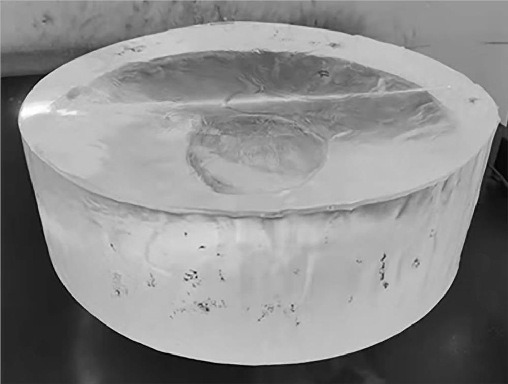
[0044] CsI:0.1 at% TlI crystals with a diameter of 330 mm were grown in a crystal growth furnace.

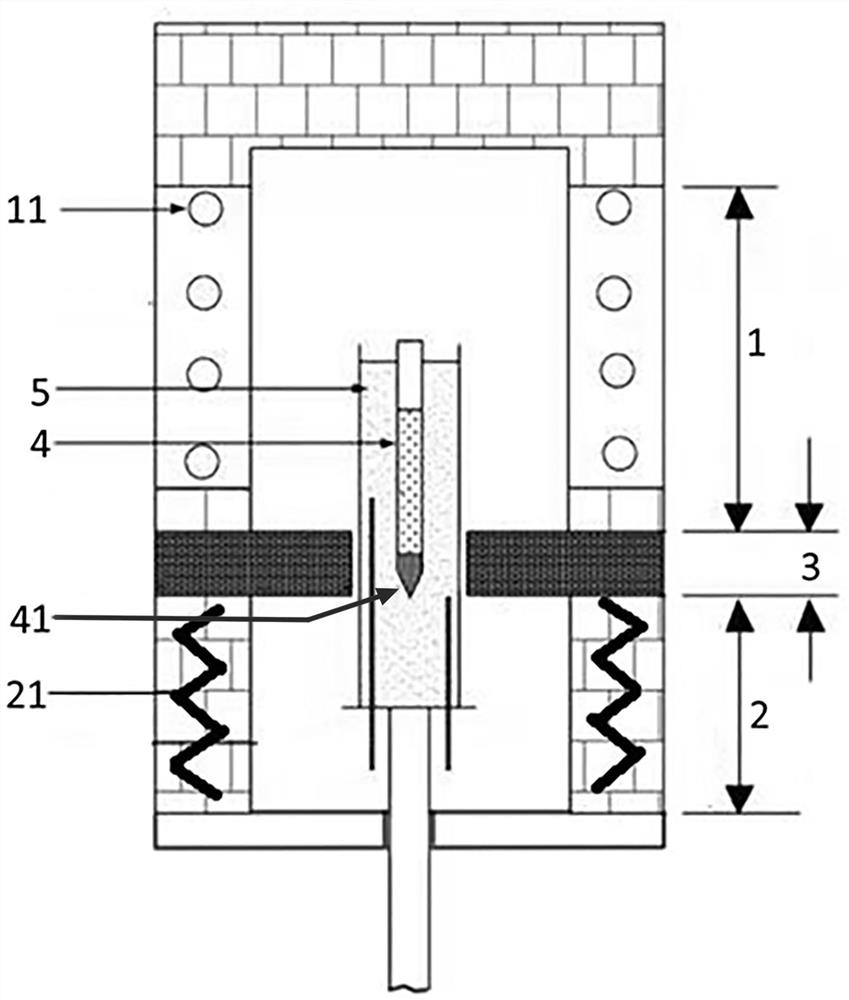
[0045] (1) Raw material preparation: thallium-doped cesium iodide crystal with Tl doping concentration of 0.1%. Using high-quality cesium iodide single crystal as the seed crystal, put the seed crystal into the narrowed section 41 at the bottom of the crucible 4 to prevent the seed crystal from shifting, then mix the raw materials into the platinum crucible, and put a lid on the top of the crucible 4 to prevent Impurities fall in. Among them, the weight of CsI (seed crystal + crystal block + powder) weighed is 49999.75 g, and the weight of TlI is 638.2 g.

[0046] (2) Crucible 4 loading: place the platinum crucible vertically in the insulation cover 5 of the crystal growth furnace and put it into the growth furnace, and the bottom of the platinum crucible is located in the crystallization area 3; Heating to a temperature of 200 °C, the vacuum degree reaches 4.5×10 -3 Pa, keep...


PUM

PropertyMeasurementUnit
Diameteraaaaaaaaaa
Thicknessaaaaaaaaaa

Abstract

The invention relates to a thallium-doped cesium iodide scintillation crystal preparation method and a radiation detection panel. The preparation method comprises the following steps: placing a raw material for forming the thallium-doped cesium iodide scintillation crystal and a seed crystal for guiding the crystallization of the raw material in a crystal growth container, and placing the crystal growth container in a non-uniform temperature field; controlling the upper temperature of the temperature field to be higher than the crystallization temperature and the lower temperature to be lower than the crystallization temperature so as to form a solid-liquid mixed state with liquid upper part and solid lower part in the crystal growth container; the crystal growth container moves downwards relative to the temperature field, and the solid-liquid interface gradually moves upwards relative to the crystal growth container, so that the solid at the bottom of the crystal growth container continuously grows to form the thallium-doped cesium iodide scintillation crystal. According to the method, the large-size thallium-doped cesium iodide scintillation crystal with the diameter of 330 mm can be prepared, and low-cost batch production of the large-size thallium-doped cesium iodide scintillation crystal is facilitated.

Description

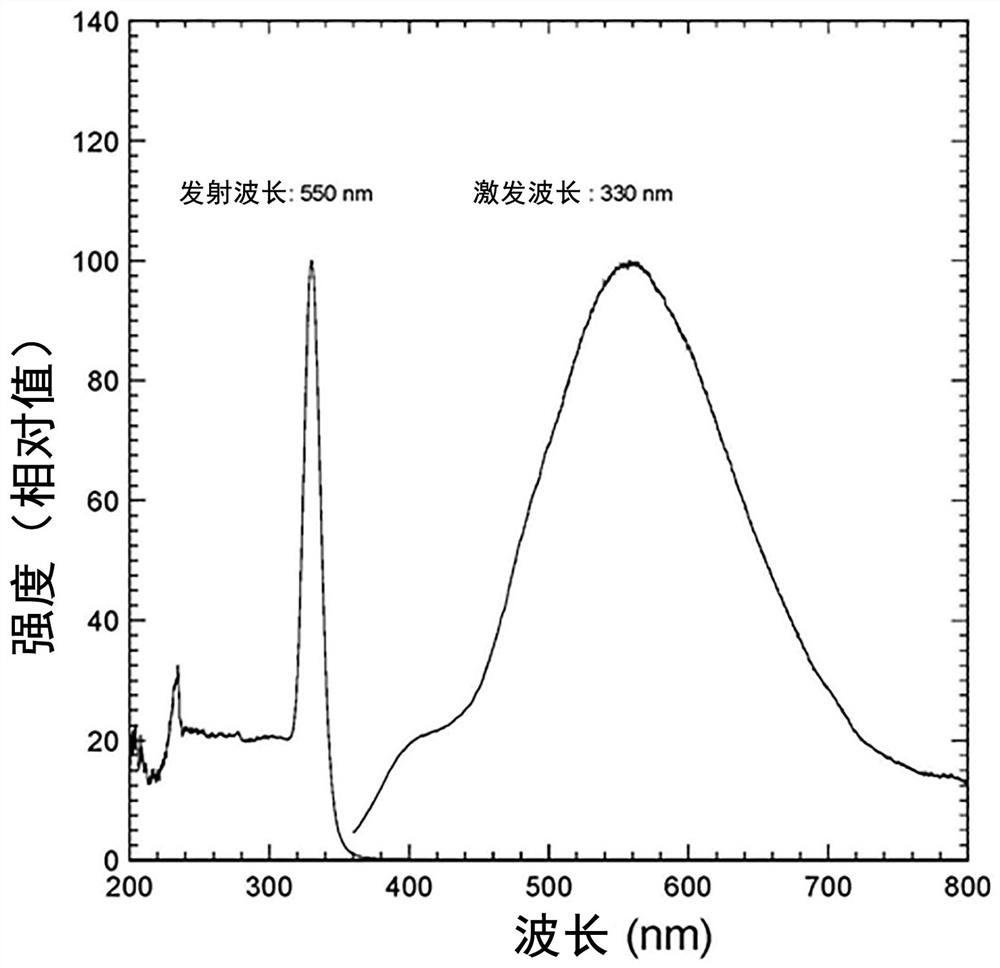
technical field [0001] The invention relates to the field of scintillation crystal manufacturing and radiation detection equipment, in particular to a preparation method of thallium-doped cesium iodide scintillation crystal and a radiation detection panel. Background technique [0002] Cesium iodide (CsI) scintillation crystals are colorless and transparent cubic crystals with a density of 4.51 g / cm3 and a Mohs hardness of 2 without cleavage. They are slightly deliquescent in air. According to different dopants, cesium iodide scintillation crystals can be divided into three types: thallium (Tl) activated, sodium (Na) activated and pure cesium iodide. After doping thallium or sodium ions in the crystal, it has high luminous efficiency under the excitation of X-rays, γ-rays or other high-energy particles. The emission wavelength is located at 550 nanometers, which can coincide with the sensitive wavelength of silicon photodiodes. Taking advantage of this characteristic, cesi...

Claims


Application Information

Patent Timeline
IPC IPC(8): C30B29/12C30B11/00G01T1/202
CPCC30B29/12C30B11/003C30B11/002C30B11/006G01T1/202
Inventor 任国浩史坚李焕英吴云涛
Owner 江苏先进无机材料研究院
Learn More