Solar cell and preparation method thereof

A solar cell and conductive type technology, applied in the field of solar energy, can solve problems such as reducing the conversion efficiency of solar cells, and achieve the effects of reducing losses, increasing effective output, and improving effective output

Pending Publication Date: 2022-05-13
一道新能源科技股份有限公司
View PDF6 Cites 0 Cited by
  • Summary
  • Abstract
  • Description
  • Claims
  • Application Information

AI Technical Summary

Problems solved by technology

The inventors of the present application have found in practice that the doped polysilicon layer in the contact structure provides field-effect passivation for the crystalline silicon itself and is responsible for forming an ohmic contact with the electrodes of the external circuit, but actually it still belongs to the photogenerated carrier of the solar cell The conductive carrier has a large number of recombination centers due to its own structural defects, which still has great restrictions on the final transfer of carriers to the external circuit, which reduces the conversion efficiency of solar cells to a certain extent.

Method used


Image

  • Solar cell and preparation method thereof
  • Solar cell and preparation method thereof
  • Solar cell and preparation method thereof

Examples


Embodiment 1

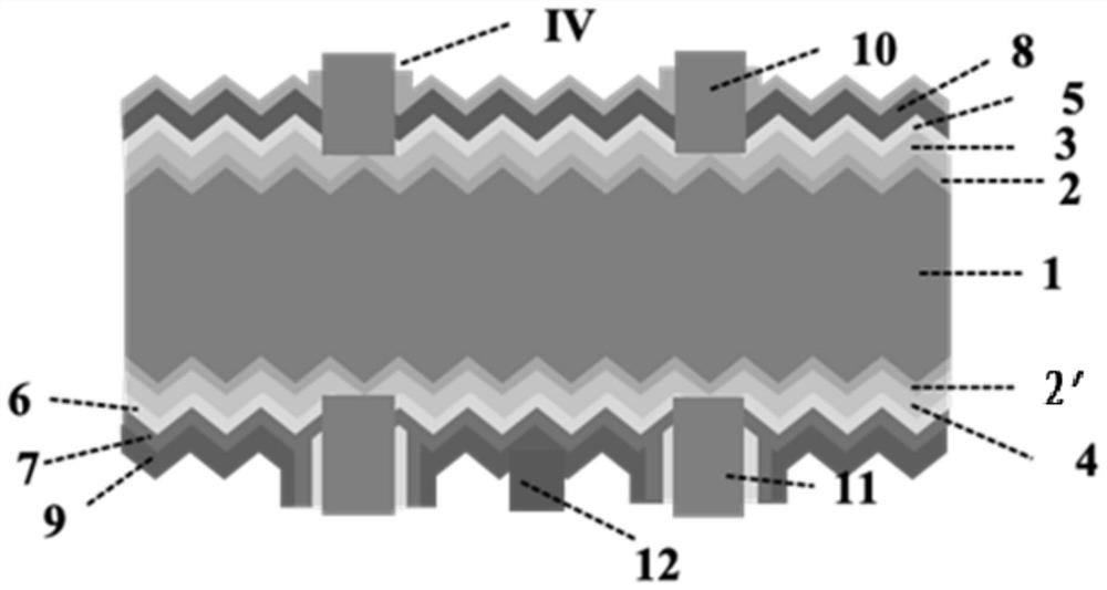
[0057] figure 1 It is a vertical cross-sectional view of a solar cell according to an embodiment of the present application.

[0058] The solar cell provided in this embodiment is a part of a solar module, that is, a component capable of generating photocurrent, and its structure includes a crystalline silicon substrate of the first conductivity type, and the crystalline silicon is single crystal silicon or polycrystalline silicon, and the so-called first conductivity type is the same as A concept corresponding to the second conductivity type that will be described below, where the first conductivity type is n-type, the second conductivity type is p-type, and if the first conductivity type is p-type, the second conductivity type is n type.

[0059] refer to figure 1 As shown, the solar cell in this application is described in detail by taking the first conductivity type as n-type as an example. The crystalline silicon substrate is an n-type crystalline silicon substrate 1, a...

Embodiment 2

[0069] This embodiment also provides a preparation method for preparing the solar cell of the previous embodiment, such as Figure 2a~2q As shown, this embodiment takes an n-type crystalline silicon substrate as an example to describe the preparation process of the solar cell as follows.

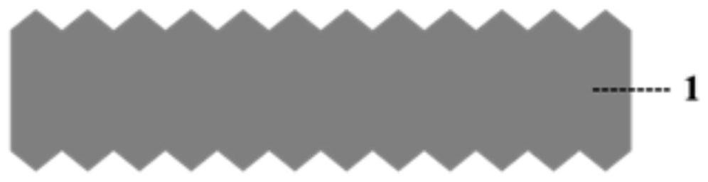
[0070] Step 1: For n-type 158.78*158.75mm with a resistivity of 0.5-3Ω.cm 2 The single crystal silicon wafer 1 is cleaned, the damaged layer is removed, and the texture is made to form a random pyramid structure on the surface of the crystal silicon wafer;

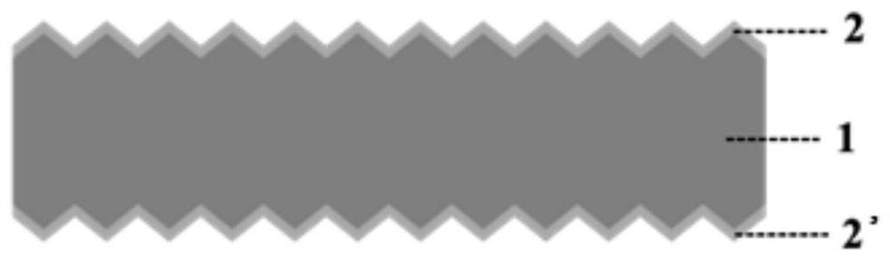
[0071] Step 2: Using the LPCVD method, the first tunneling thin film layer 2 and the second tunneling thin film layer 2' are grown on both sides of the n-type textured silicon wafer 1, and the first tunneling thin film layer and the second tunneling thin film layer are The thickness is 1-3nm;

[0072] Step 3: growing double-sided intrinsic amorphous silicon layers 3' and 4' on the tunneling thin film layer, and the thickness of the int...


PUM

PropertyMeasurementUnit
thicknessaaaaaaaaaa
thicknessaaaaaaaaaa
thicknessaaaaaaaaaa

Abstract

The embodiment of the invention provides a solar cell and a preparation method thereof, the solar cell comprises a crystalline silicon substrate, and a first tunneling film layer, a doped polycrystalline silicon layer, a first passivation layer, an anti-reflection layer and a mask layer are prepared on one surface of the crystalline silicon substrate; and a second tunneling thin film layer, a heavily doped polycrystalline silicon layer, a second passivation layer, an overweight doped polycrystalline silicon layer and a transparent conductive layer are prepared on the other surface. Good chemical passivation and field effect passivation on the surface of the doped polycrystalline silicon layer are realized by introducing the passivation layer, the loss of carriers caused by recombination on the polycrystalline silicon layer is reduced, and the effective output of photon-generated carriers is improved; through introduction of the overweight doped polycrystalline silicon layer, field effect passivation of one surface is further enhanced, certain power is provided for output of photon-generated carriers to an external circuit through potential difference values generated by different doping concentrations, effective output of the carriers is increased again, and therefore the conversion efficiency of the solar cell is effectively improved.

Description

technical field [0001] The invention relates to the technical field of solar energy, in particular to a solar cell and a preparation method thereof. Background technique [0002] Crystalline silicon solar cells are the most mature and widely used solar cells, accounting for more than 90% of the photovoltaic market, and will occupy a dominant position for a long time in the future. Among the many factors affecting the photoelectric conversion efficiency of crystalline silicon solar cells, the recombination of the contact between metal electrodes and crystalline silicon is the key factor, which is considered to be the last limiting factor close to the theoretical limit efficiency. At present, the use of a tunnel oxide layer to passivate the metal contact structure can significantly reduce the recombination of the metal contact area, and at the same time have good contact performance, which can greatly improve the conversion efficiency of crystalline silicon solar cells. Compa...

Claims


Application Information

Patent Timeline
Patent Type & Authority Applications(China)
IPC IPC(8): H01L31/068H01L31/0216H01L31/0224H01L31/18
CPCH01L31/068H01L31/02167H01L31/02168H01L31/022425H01L31/1804H01L31/1868Y02E10/547
Inventor 王洪喆刘勇朴松源潘强强李家栋杨刘
Owner 一道新能源科技股份有限公司
Why Eureka
Try Eureka