Dry etching process of N-polarity III-V group semiconductor material
A III-V, dry etching technology, applied in semiconductor/solid-state device manufacturing, climate sustainability, sustainable manufacturing/processing, etc., can solve the problem of increased etching surface roughness, process and device preparation effects, etc. question
- Summary
- Abstract
- Description
- Claims
- Application Information
AI Technical Summary
Problems solved by technology
Method used
Image

Examples
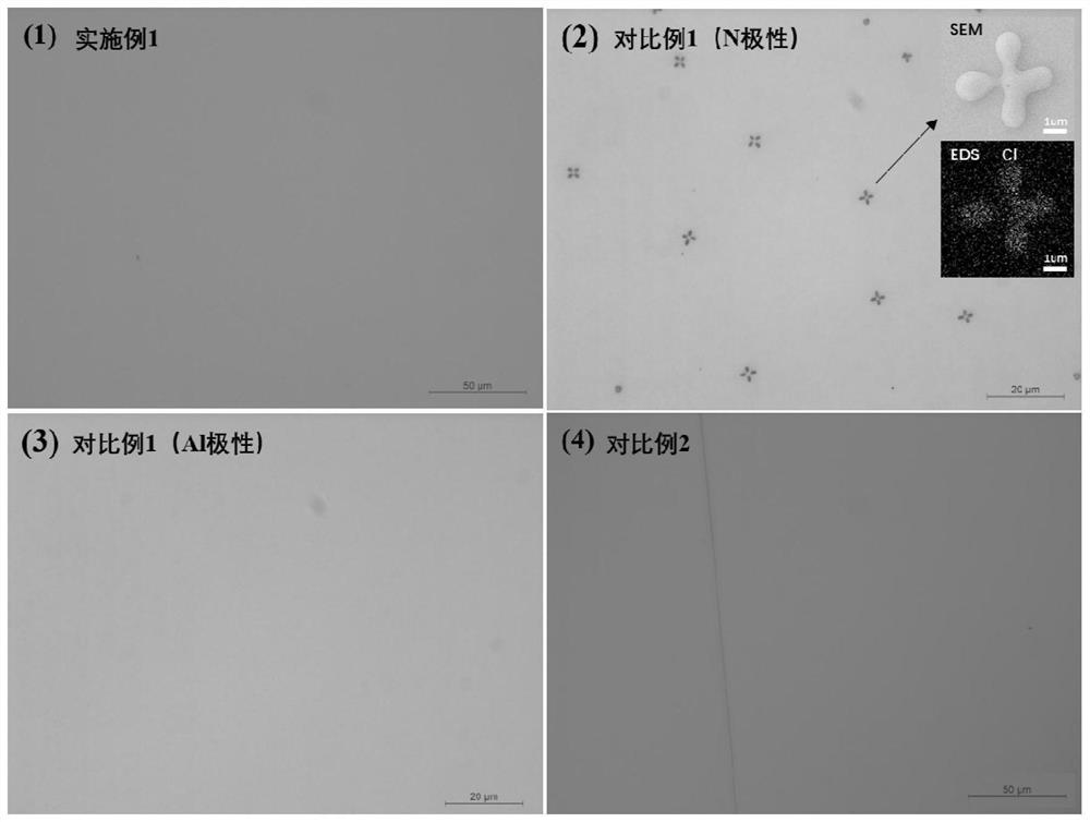
Embodiment 1
[0026] An embodiment of the dry etching process of the present invention, the dry etching process of this embodiment includes the following steps:
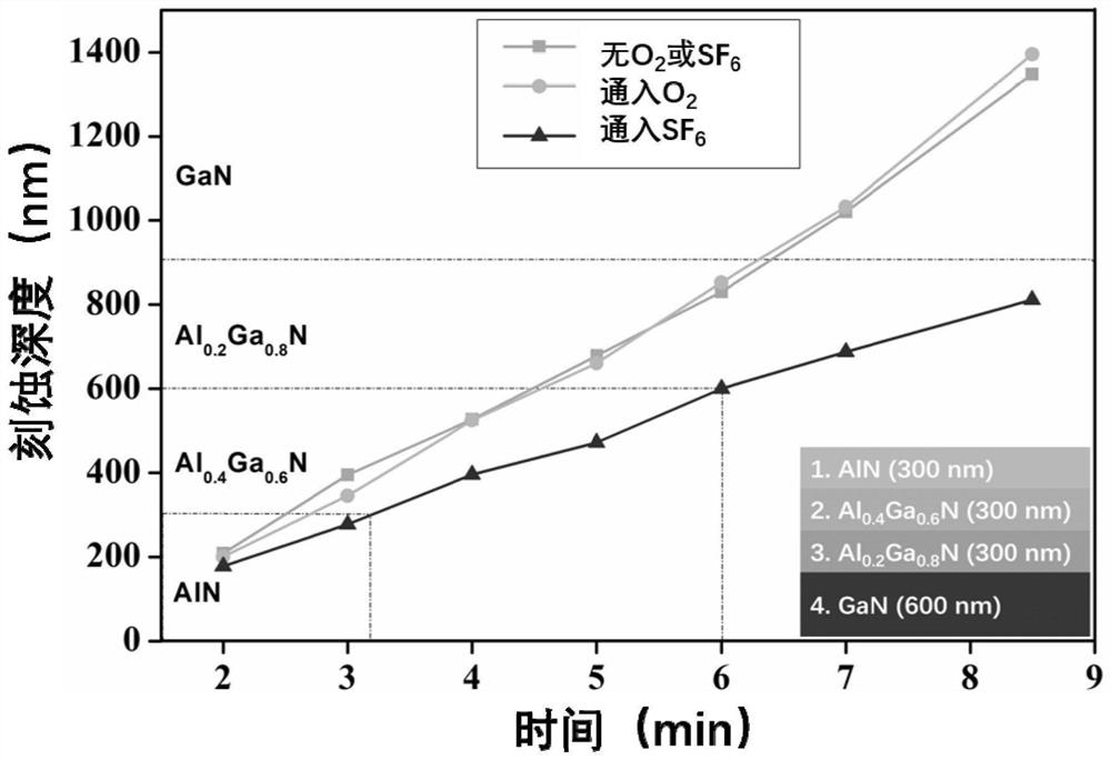
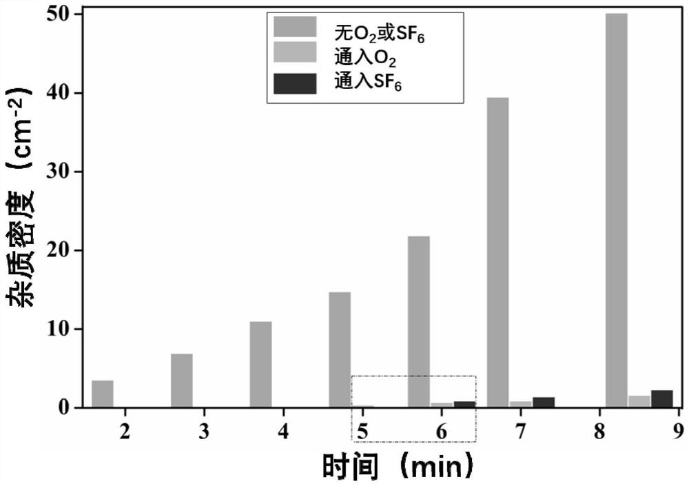
[0027] (1) The etching object is N-polar Al(Ga)N thin film material, which is divided into four layers from top to bottom, AlN, Al in turn 0.4 Ga 0.6 N, Al 0.2 Ga 0.8 N, GaN, the thickness of each layer is 300nm; ultrasonically clean the etched objects with acetone, isopropanol and deionized water respectively, and dry them with nitrogen;
[0028] (2) Put the etched object into the reaction chamber of the ICP etching machine, and feed 8sccm of BCl 3 , 24sccm of Cl 2 , Ar of 5sccm, SF of 3sccm 6 , the pressure in the chamber is 8mtorr, the sample temperature is 20℃, the ICP power is 500W, and the RF bias power is 150W.
Embodiment 2
[0030] An embodiment of the dry etching process of the present invention, the dry etching process of this embodiment includes the following steps:
[0031] (1) The sample is an N-polar Al(Ga)N thin film material, which is divided into four layers from top to bottom, AlN, Al in turn 0.4 Ga 0.6 N, Al 0.2 Ga 0.8 N, GaN, the thickness of each layer is 300nm; ultrasonically clean the etched objects with acetone, isopropanol and deionized water respectively, blow dry with nitrogen, and then bake on a hot plate at 110°C for 10min;
[0032] (2) Spin coating, pre-bake, expose, develop, and post-bake the above samples using AZ 4620 photoresist to obtain an etching preparation sheet; spin coating rate 8000rps, time 30s; prebaking temperature 105°C, time 90s; exposure Time 8s; development time 3min; post-baking temperature 105℃, time 3min;
[0033] (3) Put the etched object into the reaction chamber of the ICP etching machine, and feed 8sccm of BCl 3, 24sccm of Cl 2 , Ar of 5sccm, S...
Embodiment 3
[0036] An embodiment of the dry etching process of the present invention, the dry etching process of this embodiment includes the following steps:
[0037] (1) The etching object is N-polar Al(Ga)N thin film material, which is divided into four layers from top to bottom, AlN, Al in turn 0.4 Ga 0.6 N, Al 0.2 Ga 0.8 N, GaN, the thickness of each layer is 300nm; ultrasonically clean the etched objects with acetone, isopropanol and deionized water respectively, and dry them with nitrogen;
[0038] (2) Put the etched object into the reaction chamber of the ICP etching machine, and feed 5sccm of BCl 3 , 30sccm of Cl 2 , Ar of 10sccm, SF of 2sccm 6 , the pressure in the chamber is 8mtorr, the sample temperature is 20℃, the ICP power is 500W, and the RF bias power is 150W.
PUM
| Property | Measurement | Unit |
|---|---|---|
| surface roughness | aaaaa | aaaaa |
| surface roughness | aaaaa | aaaaa |
| surface roughness | aaaaa | aaaaa |
Abstract
Description
Claims
Application Information
 - R&D
- Intellectual Property
- Life Sciences
- Materials
- Tech Scout
- Unparalleled Data Quality
- Higher Quality Content
- 60% Fewer Hallucinations
Browse by: Latest US Patents, China's latest patents, Technical Efficacy Thesaurus, Application Domain, Technology Topic, Popular Technical Reports.
© 2025 PatSnap. All rights reserved.Legal|Privacy policy|Modern Slavery Act Transparency Statement|Sitemap|About US| Contact US: help@patsnap.com