Supercharge Your Innovation With Domain-Expert AI Agents!

Light emitting diode epitaxial wafer and preparation method thereof

A technology of light-emitting diodes and epitaxial wafers, applied in semiconductor devices, electrical components, circuits, etc., can solve problems such as lattice mismatch and reduce the luminous efficiency of light-emitting diode epitaxial wafers, so as to reduce the degree of influence, facilitate strain relaxation, The effect of enhancing limited abilities

Active Publication Date: 2022-06-17
JIANGXI ZHAO CHI SEMICON CO LTD
View PDF8 Cites 3 Cited by
  • Summary
  • Abstract
  • Description
  • Claims
  • Application Information

AI Technical Summary

Problems solved by technology

[0005] Based on this, the purpose of the present invention is to provide a light-emitting diode epitaxial wafer and its preparation method to fundamentally solve the problems caused by the lattice mismatch between the existing P-type electron blocking layer and the multi-quantum well layer and the P-type GaN layer. The problem of reducing the luminous efficiency of light-emitting diode epitaxial wafers

Method used


Image

  • Light emitting diode epitaxial wafer and preparation method thereof
  • Light emitting diode epitaxial wafer and preparation method thereof
  • Light emitting diode epitaxial wafer and preparation method thereof

Examples


Embodiment 1

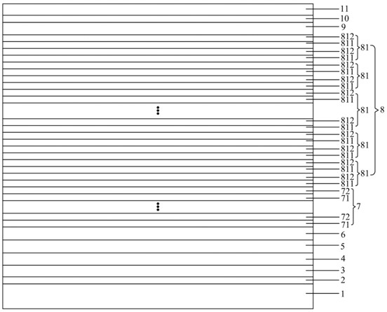
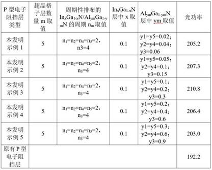
[0038] see figure 1, is a schematic structural diagram of a light-emitting diode epitaxial wafer provided by an embodiment of the present invention. For the convenience of description, only the part related to the embodiment of the present invention is shown. The light-emitting diode epitaxial wafer provided by the embodiment of the present invention includes: a substrate 1 , and a buffer layer 2, a three-dimensional nucleation layer 3, a two-dimensional recovery layer 4, an undoped GaN layer 5, an N-type GaN layer 6, a multiple quantum well layer 7, and a P-type electron blocking layer stacked in sequence on the substrate 1 layer 8, P-type undoped GaN layer 9, P-type Mg-doped GaN layer 10 and P-type contact layer 11; wherein the P-type electron blocking layer 8 includes m superlattice structure sublayers 81; Layer 81 is composed of n m A periodically arranged In x Ga 1-x N / Al ym Ga 1-ym A superlattice structure composed of N; along the direction from the multiple quantum...

Embodiment 2

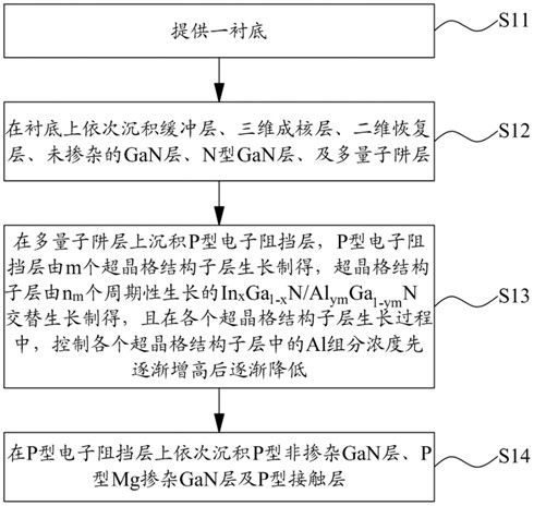
[0067] see figure 2 , which shows a method for preparing a light-emitting diode epitaxial wafer in the second embodiment of the present invention, and the method specifically includes steps S11 to S14 .

[0068] Step S11, providing a substrate.

[0069] Wherein, in this embodiment of the present invention, the selected substrate may be any one of a sapphire substrate, a silicon substrate, a silicon carbide substrate, and a gallium nitride substrate. Specifically, in this embodiment, sapphire is used as the substrate. The epitaxial layer growth substrate, which may specifically be a patterned sapphire substrate or a sapphire flat substrate.

[0070] Further, the present invention uses metal organic chemical vapor deposition (MOCVD) equipment to grow epitaxial wafers. Among them, high-purity ammonia (NH 3 ) as N (nitrogen) source, trimethylgallium (TMGa) and triethylgallium (TEGa) as Ga (gallium) source, trimethylindium (TMIn) as In (indium) source, trimethylaluminum (TMAl) ...


PUM

PropertyMeasurementUnit
Thicknessaaaaaaaaaa
Thicknessaaaaaaaaaa
Thicknessaaaaaaaaaa

Abstract

The invention provides a light-emitting diode epitaxial wafer and a preparation method thereof. The light-emitting diode epitaxial wafer comprises a substrate, and a buffer layer, a three-dimensional nucleating layer, a two-dimensional recovery layer, an undoped GaN layer, an N-type GaN layer, a multi-quantum well layer, a P-type electron barrier layer, a P-type non-doped GaN layer, a P-type Mg-doped GaN layer and a P-type contact layer which are sequentially stacked on the substrate, the P-type electron barrier layer comprises m superlattice structure sub-layers; the superlattice structure sublayer is of a superlattice structure composed of nm pieces of In < x > Ga < 1-x > N / Al < y > m Ga < 1-y > m N which are arranged periodically. Along the direction from the multi-quantum well layer to the P-type non-doped GaN layer, the concentration of the Al component in each superlattice structure sub-layer is gradually increased and then gradually reduced. The light-emitting diode epitaxial wafer solves the problem that the light-emitting efficiency of the light-emitting diode epitaxial wafer is reduced due to lattice mismatch between the existing P-type electron barrier layer and the multi-quantum well layer and between the existing P-type electron barrier layer and the P-type GaN layer.

Description

technical field [0001] The invention relates to the field of optoelectronic technology, in particular to a light-emitting diode epitaxial wafer and a preparation method thereof. Background technique [0002] Light-emitting diodes (LEDs) are commonly used light-emitting devices that emit energy through the recombination of electrons and holes, and are widely used in the field of lighting. Light-emitting diodes can efficiently convert electrical energy into light energy, and have a wide range of uses in modern society, such as lighting, flat panel displays, medical devices, etc. With the continuous development of LED technology, while it is more and more widely used, it also faces higher and higher requirements, especially the luminous efficiency and antistatic performance of LEDs. [0003] At present, the luminous efficiency of LEDs is still not high, especially as the chip size decreases, the current density becomes larger and larger, and the electrons have lower effective ...

Claims


Application Information

Patent Timeline
IPC IPC(8): H01L33/14H01L33/06H01L33/32H01L33/00
CPCH01L33/14H01L33/06H01L33/325H01L33/007
Inventor 侯合林谢志文张铭信陈铭胜
Owner JIANGXI ZHAO CHI SEMICON CO LTD
Features
  • R&D
  • Intellectual Property
  • Life Sciences
  • Materials
  • Tech Scout
  • Unparalleled Data Quality
  • Higher Quality Content
  • 60% Fewer Hallucinations
Learn More