Preparation method of large-area uniform single-layer graphene film
A technology of single-layer graphene and multi-layer graphene, which is applied in the field of graphene and can solve the problems of large-area, uniform, and high-quality single-layer graphene
- Summary
- Abstract
- Description
- Claims
- Application Information
AI Technical Summary
Problems solved by technology
Method used
Image
Examples
Embodiment 1
[0055] Example 1. Preparation of large-area continuous single-layer graphene film
[0056] 1) Preparation of large-area monolayer continuous graphene films
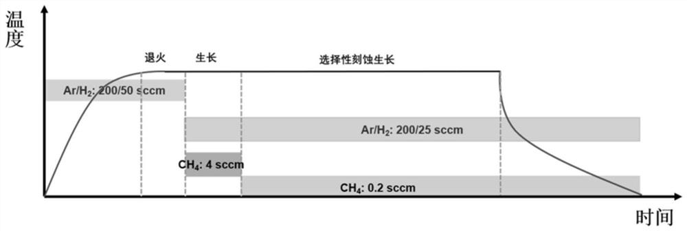
[0057] The large-area single crystal copper (111) was electrochemically polished, the sample copper foil with a thickness of 100 μm was connected to the positive electrode of the DC power supply, and the metal copper electrode was connected to the negative electrode. The applied voltage is 2-6V, preferably 5V, the current is 1-4A, preferably 3A, and the polishing time is 2-5min, preferably 3min. Then rinse with deionized water, normal N 2 Blow dry. , placed in the center of the tube furnace, passed 200sccm of argon and 25sccm of hydrogen, set the heating time to 45min, when the temperature reached 1075 ℃, passed 4sccm of methane and grown for 1h.
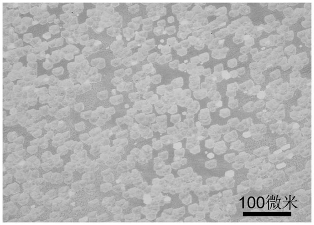
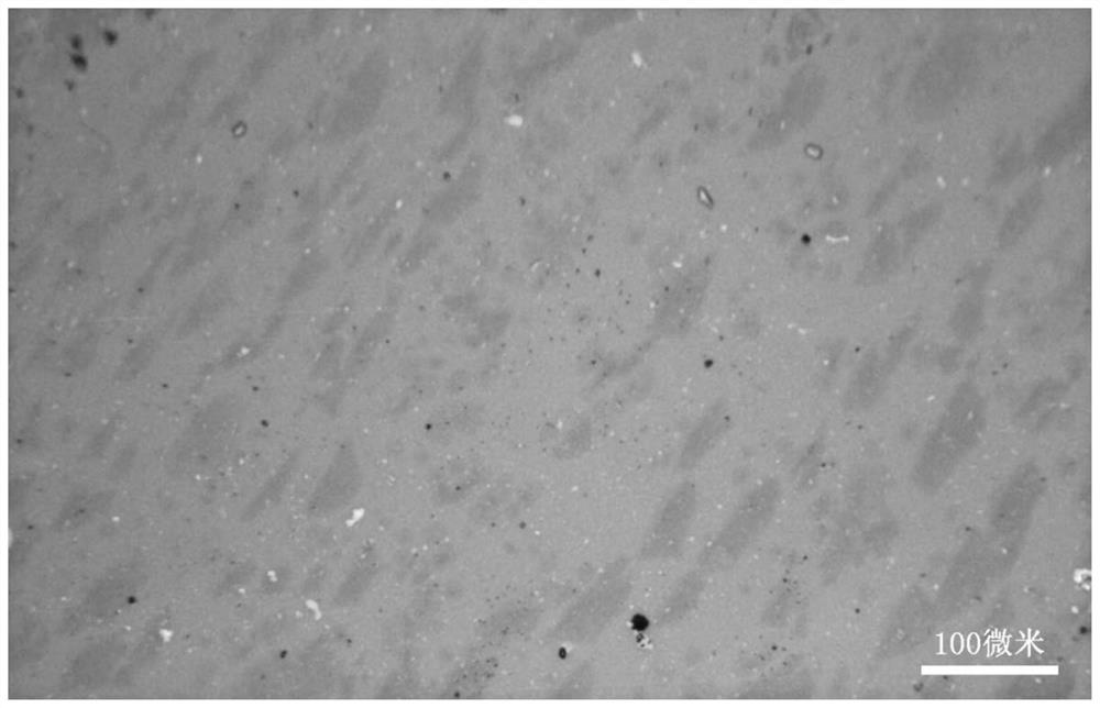
[0058] During this process, graphene islands will form oriented, multi-layer graphene single crystals on the surface of copper (111), such as figure 1 shown. With the prog...
PUM
| Property | Measurement | Unit |
|---|---|---|
| thickness | aaaaa | aaaaa |
Abstract
Description
Claims
Application Information


