Selective emitter structure, its preparation method and application

An emitter and selective technology, applied in photovoltaic power generation, climate sustainability, final product manufacturing, etc., can solve the problem of battery open circuit voltage and fill factor, metal diffusion into the interior of monocrystalline silicon, equipment and pipeline life effects, etc. problem, achieve the effect of reducing carrier recombination, excellent passivation effect, and avoiding the existence of high recombination area

Active Publication Date: 2022-03-08
NINGBO INST OF MATERIALS TECH & ENG CHINESE ACADEMY OF SCI
View PDF0 Cites 0 Cited by
  • Summary
  • Abstract
  • Description
  • Claims
  • Application Information

AI Technical Summary

Problems solved by technology

However, there are some defects in the existing preparation process of this type of solar cell, for example: when firing the front gate electrode, the silver paste will penetrate the anti-reflection layer and passivation layer, contact with single crystal silicon, and achieve a good electrode touch
However, despite the continuous optimization of the area and preparation method of the gate finger electrode, the direct contact between the metal and the single crystal silicon still exists, which will also introduce significant metal contact recombination damage, making it difficult to further improve the open circuit voltage and fill factor of the battery.
Specifically, the hazards of direct contact between metal electrodes and single crystal silicon are at least: ① resulting in a large number of interface states and serious carrier recombination. Generally speaking, the saturation current density of the metal-to-metal contact area is 2000fA / cm 2 above, thus seriously affecting the efficiency of the battery; ②The metal may diffuse into the single crystal silicon, resulting in serious recombination of carriers in the body
[0003] The current main method to reduce metal contact compound damage is to use selective emitter, that is, to use laser ablation of phosphosilicate glass or borosilicate glass to form local heavy doping during the ablation process, but the ablation process will bring surface damage layer, resulting in a large recombination current, J 0,met Probably at 1000fA / cm 2 about
In addition, there are many technical problems in the process and equipment of the commonly used boron-expanded emitters, mainly in the following aspects: 1) If BBr is used 3 As a diffusion source, it is easy to produce viscous by-products containing bromine in the furnace door area during the reaction process, resulting in sticking of the furnace door; 2) If BCl is used instead 3 To avoid sticking of the furnace door, HCl or Cl will be produced 2 Such strong corrosive by-products will seriously affect the life of equipment and pipelines

Method used


Image

  • Selective emitter structure, its preparation method and application
  • Selective emitter structure, its preparation method and application
  • Selective emitter structure, its preparation method and application

Examples


preparation example Construction

[0062] In some embodiments, the preparation method further includes: forming the first dielectric layer on the surface of the silicon substrate by at least any one of oxidation, physical or chemical deposition, but not limited thereto. The oxidation method includes but not limited to wet chemical oxidation method, high temperature oxidation method, plasma assisted oxidation method, ozone oxidation method or other surface oxidation methods and the like. The physical or chemical deposition methods include, but are not limited to, plasma-assisted atomic layer deposition, plasma-enhanced chemical vapor deposition (PECVD), low-pressure chemical vapor deposition (LPCVD), and the like.

[0063] In some embodiments, the preparation method further includes: at least a chemical vapor deposition method or a physical vapor deposition method combined with an in-situ doping method or a secondary doping method can be selected to form a preparation method on the first dielectric layer. A heav...

Embodiment 1

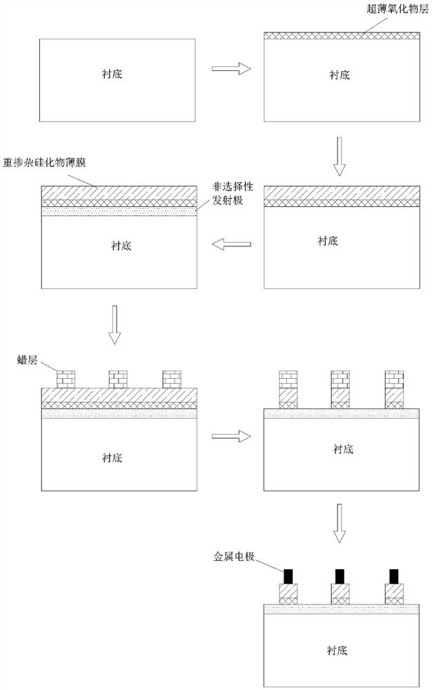
[0087] Embodiment 1 The preparation method of a selective emitter structure provided in this embodiment includes the following steps:

[0088] (1) Cleaning and double-sided alkali polishing of n-type silicon wafers;

[0089] (2) Using PECVD in-situ oxidation method to prepare ultra-thin silicon oxide layers (thickness greater than 0 and less than 3nm) on both the front and back sides of the silicon wafer;

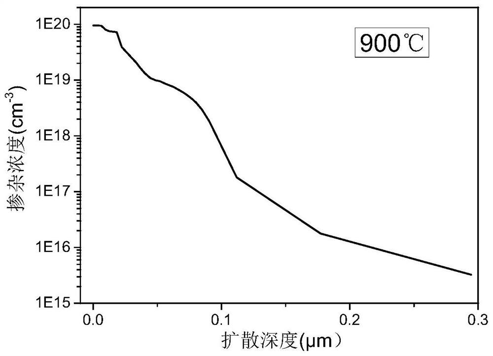
[0090] (3) Prepare a boron-doped amorphous silicon oxide film with a thickness of 60-300 nm on the front and back sides of the silicon wafer by PECVD method (wherein the boron atomic concentration is 1E17 cm -3 ~5E20cm -3 , the oxygen atomic concentration is 0.1at%~50at%, and the oxygen content on the side near the surface of the silicon wafer is low, and the oxygen content on the side away from the surface of the silicon wafer is high), and then at 900°C to 1000°C with multiple different annealing times ( 1min~600min) for high temperature annealing to form a boron-doped ...

Embodiment 2

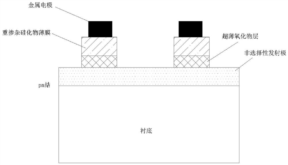
[0103] Embodiment 2 refers to Figure 4 As shown, the n-TOPCon crystalline silicon cell based on an n-type silicon chip provided by this embodiment includes an n-type silicon chip, the front side of the n-type silicon chip is covered with a p-type boron-doped emitter, and the boron-doped emitter Several selective emitter structures are distributed on the electrode, wherein the selective emitter structure includes an ultra-thin silicon oxide layer and a boron-doped polysilicon oxide layer stacked in sequence, and the boron-doped polysilicon oxide layer is combined with a metal electrode (defined as the first An electrode), and the selective emitter structure and the boron-doped emitter are also covered with an aluminum oxide layer and a silicon nitride layer in sequence, and the first electrode is exposed from the aluminum oxide layer and the silicon nitride layer. A diffusion doped layer is formed on the back side of the n-type silicon wafer, and an ultra-thin silicon oxide la...


PUM

PropertyMeasurementUnit
thicknessaaaaaaaaaa
thicknessaaaaaaaaaa
thicknessaaaaaaaaaa

Abstract

The invention discloses a selective emitter structure, its preparation method and application. The selective emitter structure includes a first dielectric layer and a heavily doped silicide layer sequentially stacked on the surface of a crystalline silicon cell substrate, and a metal electrode as a first electrode is combined on the heavily doped silicide layer. In the present invention, by applying the aforementioned selective emitter structure to the front of the crystalline silicon solar cell, the contact between the metal electrode and the single crystal silicon substrate can be eliminated, the existence of a high recombination zone can be avoided, the recombination of carriers can be reduced, and a more excellent The passivation effect, and also improve the carrier collection efficiency, can obtain lower contact resistivity, thereby optimizing the battery performance, improving the battery efficiency, in addition to simplifying the manufacturing process of crystalline silicon solar cells, reducing the manufacturing cost.

Description

technical field [0001] The invention relates to a preparation process of a selective emitter structure, in particular to a selective emitter structure based on a silicon oxide / doped polycrystalline silicide laminated structure and its preparation method and application, belonging to the field of semiconductor technology. Background technique [0002] Tunnel Oxide Passivated-Contact Structures (TOPCon, Tunnel Oxide Passivated-Contact structures) is a new crystalline silicon solar cell structure proposed in 2014, aiming to improve the passivation of the back of the silicon cell. Specifically, this technology uses an n-type silicon wafer, first grows a layer of ultra-thin silicon oxide with a thickness of less than 3nm on the back of the silicon wafer, then deposits a layer of phosphorus-doped amorphous silicon or polysilicon layer, and finally prepares a full back metal electrodes. The main advantage of the TOPCon structure is that it realizes the comprehensive passivation of...

Claims


Application Information

Patent Timeline
Patent Type & Authority Patents(China)
IPC IPC(8): H01L31/068H01L31/0224H01L31/18
CPCH01L31/068H01L31/022425H01L31/1804H01L31/1868Y02E10/547Y02P70/50
Inventor 曾俞衡叶继春闫宝杰刘尊珂廖明墩程皓林毅然郑晶茗卢琳娜智雨燕冯蒙蒙
Owner NINGBO INST OF MATERIALS TECH & ENG CHINESE ACADEMY OF SCI
Why Eureka
Try Eureka