Light-emitting device and preparation method thereof

A technology for light-emitting devices and quantum dots to emit light, which is applied in the manufacture of semiconductor/solid-state devices, semiconductor devices, and electric solid-state devices, etc. It can solve problems affecting electron injection efficiency, charge accumulation, poor interface fusion, etc. Interface gap optimization, good interface bonding performance

Pending Publication Date: 2022-07-01
TCL CORPORATION
View PDF0 Cites 0 Cited by
  • Summary
  • Abstract
  • Description
  • Claims
  • Application Information

AI Technical Summary

Problems solved by technology

[0004] The purpose of the present application is to provide a light-emitting device and its preparation method, aiming to solve the problem of poor interface fusion between the electron transport layer and the adjacent functional layer, which affects the electron injection efficiency and is easy to form charge accumulation.

Method used


Image

  • Light-emitting device and preparation method thereof
  • Light-emitting device and preparation method thereof
  • Light-emitting device and preparation method thereof

Examples


preparation example Construction

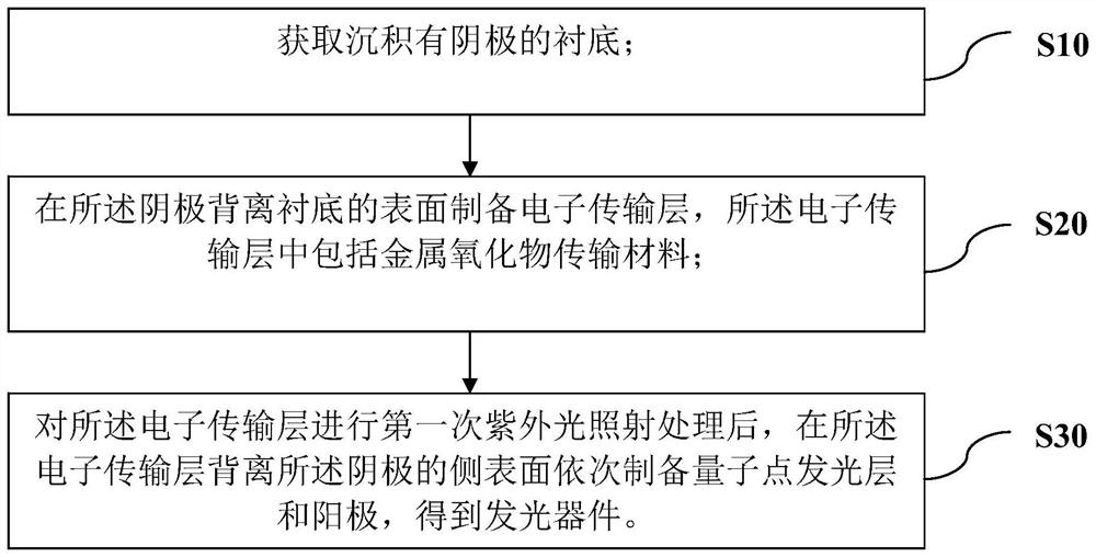
[0023] as attached figure 1 As shown, the first aspect of the embodiments of the present application provides a method for preparing a light-emitting device, including the following steps:

[0024] S10. Obtain the substrate on which the cathode is deposited;

[0025] S20. Prepare an electron transport layer on the surface of the cathode away from the substrate, and the electron transport layer includes a metal oxide transport material;

[0026] S30. After the first ultraviolet light irradiation treatment is performed on the electron transport layer, a quantum dot light-emitting layer and an anode are sequentially prepared on the side surface of the electron transport layer away from the cathode to obtain a light-emitting device.

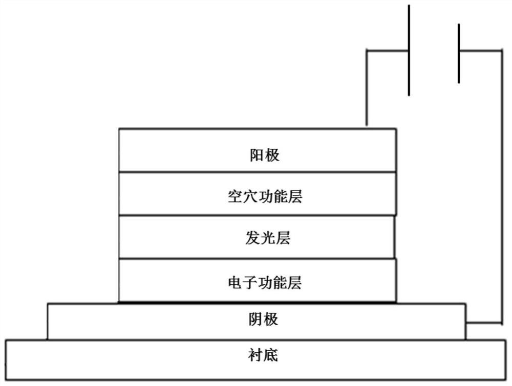
[0027] In the method for preparing a light-emitting device provided by the first aspect of the present application, after a metal oxide electron transport layer is prepared on the surface of the cathode, the electron transport layer is subjected to ...

Embodiment 1

[0076] A light-emitting diode, comprising the following preparation steps:

[0077] (1) Provide a substrate on which Al cathode is deposited, and perform pre-cleaning treatment on the substrate.

[0078] (2) forming an electron transport layer on the Al cathode of step (1): in a glove box (water oxygen content is less than 0.1 ppm), spin-coat ZnO solution (concentration is 45 mg / mL, solvent is ethanol) on the ITO cathode , spin coating at 3000rpm for 30s and then anneal at 80℃ for 30min to form an electron transport layer.

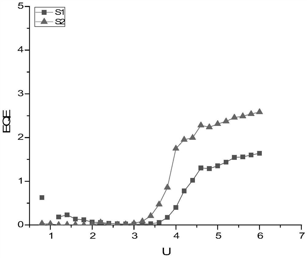
[0079] (3) in H 2 The O content is less than 1 ppm and the temperature is 100°C, the electron transport layer is irradiated vertically from the electron transport layer side, UV wavelength 400nm, intensity 100mJ / cm 2 , UV time 30min.

[0080] (4) Form the light-emitting layer on the electron transport layer: take the CdSe / ZnS quantum dot solution (concentration is 30mg / mL, the solvent is n-octane), put the CdSe / ZnS quantum dot solution in a glove box (w...

Embodiment 2

[0086] A light-emitting diode, the difference between its preparation steps and Example 1 is: in step (3), vertical UV irradiation is performed from the cathode side, the UV wavelength is 300nm, and the intensity is 200mJ / cm 2 , UV time 30min.


PUM

PropertyMeasurementUnit
wavelengthaaaaaaaaaa
particle diameteraaaaaaaaaa
thicknessaaaaaaaaaa

Abstract

The invention belongs to the technical field of display equipment, and particularly relates to a preparation method of a light-emitting device, which comprises the following steps: acquiring a substrate deposited with a cathode; preparing an electron transport layer on the surface, away from the substrate, of the cathode, wherein the electron transport layer comprises a metal oxide transport material; and after carrying out first ultraviolet irradiation treatment on the electron transport layer, sequentially preparing a quantum dot light-emitting layer and an anode on the side surface, deviating from the cathode, of the electron transport layer to obtain the light-emitting device. According to the preparation method of the light-emitting device, after the metal oxide electron transport layer is prepared on the surface of the cathode, fusion of the metal oxide electron transport material and the electrode is promoted through ultraviolet irradiation treatment, the potential barrier is reduced, and the electron injection efficiency is improved. Meanwhile, internal bonding and crystal re-growth in the electron transport layer are promoted, so that the surface of the electron transport layer is smoother, the interface roughness is reduced, the interface gap is optimized, and the influence of charge accumulation on the service life of the device is avoided.

Description

technical field [0001] The present application belongs to the technical field of display devices, and in particular, relates to a light-emitting device and a preparation method thereof. Background technique [0002] Quantum dots are nanocrystalline particles with a radius smaller than or close to the Bohr exciton radius, and their size and diameter are generally between one. Quantum dots have quantum confinement effect and can emit fluorescence when excited. Moreover, quantum dots have unique luminescence characteristics such as wide excitation peak, narrow emission peak, and tunable luminescence spectrum, which make quantum dot materials have broad application prospects in the field of photoelectric luminescence. Quantum dot light-emitting diode (QLED) is a new type of display technology that has emerged rapidly in recent years. Quantum dot light-emitting diode is a device that uses colloidal quantum dots as the light-emitting layer. The quantum dot light-emitting layer is...

Claims


Application Information

Patent Timeline
Patent Type & Authority Applications(China)
IPC IPC(8): H01L51/50H01L51/56
CPCH10K50/115H10K50/16H10K2102/00H10K71/00H10K50/00
Inventor 王天锋
Owner TCL CORPORATION
Why Eureka
Try Eureka