Preparation method of surface-enhanced Raman substrate with semiconductor oxide nanoparticle modified noble metal nanocone array structure

A surface-enhanced Raman and array structure technology, which is applied in Raman scattering, metal material coating technology, and final product manufacturing, can solve the problems of difficult preparation, difficult cost control, and poor uniformity and regularity of the morphology and structure. Simplified process steps, low cost, uniform and controllable morphology

Pending Publication Date: 2022-07-08
GRIMAT ENG INST CO LTD
View PDF1 Cites 0 Cited by
  • Summary
  • Abstract
  • Description
  • Claims
  • Application Information

AI Technical Summary

Problems solved by technology

Although this kind of noble metal and semiconductor composite nanostructure SERS substrate shows a good Raman enhancement effect, the preparation process mentioned is cumbersome and time-consuming, the morphology and structure are poor in uniformity and regularity, it is difficult to prepare a large area, and the cost is difficult to effectively control.

Method used


Image

  • Preparation method of surface-enhanced Raman substrate with semiconductor oxide nanoparticle modified noble metal nanocone array structure

Examples


preparation example Construction

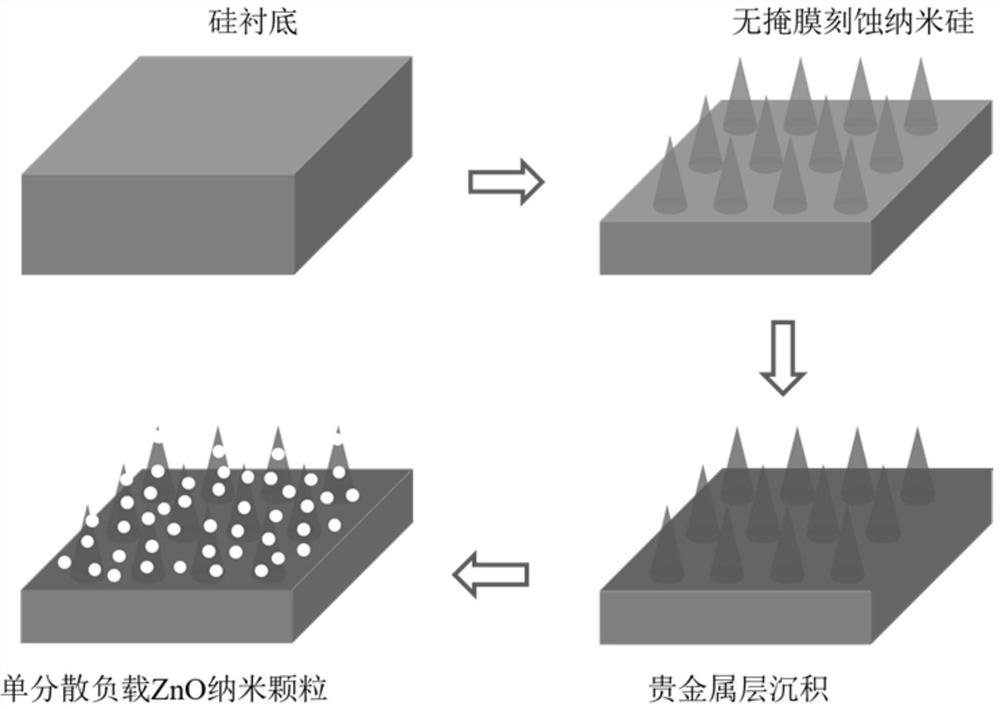
[0021] -The present invention provides a preparation method of a surface-enhanced Raman substrate with a semiconductor oxide nanoparticle modified noble metal nanocone array structure, comprising:

[0022] The first step is to prepare the substrate of the nanocone array structure;

[0023] The second step is to deposit a nanometer-thick noble metal film on the surface of the nanocone array structure;

[0024] The third step is to prepare semiconductor oxide nanoparticles, which are monodispersed and supported on the surface of the nanocone array structure 。 -

[0025] The first step is further specifically to use a low temperature inductively coupled plasma enhanced reactive ion etching technology (ICP-RIE) to perform maskless etching on the silicon wafer to obtain a large-area high-density nanocone array structure substrate.

[0026] In the first step, the reactive gas used in etching is SF 6 and O 2 , the reaction pressure is 0.5~10Pa, the reaction power is 20~80W, and t...

Embodiment 1

[0033] (1) Select 4-inch silicon wafer and configure concentrated H 2 SO 4 :H 2 O 2 Mix the cleaning solution, immerse the silicon wafer in it, cook at 120°C for 2 hours, remove the oil stains and other contaminants on the surface of the silicon wafer, rinse with ultrapure water, N 2 Blow dry spare;

[0034] (2) Use ICP-RIE technology to perform maskless etching on the surface of the cleaned silicon wafer, and use SF as the reaction gas 6 and O 2 , the reactive gas SF 6 The flow is 60sccm, O 2 The flow rate was 10sccm, the reaction pressure was 1Pa, the reaction power was 30W, and the etching time was 60s.

[0035] (3) A 50nm thick gold film was plated on the above nano-silicon cone array structure by magnetron sputtering technology, the pressure was 2Pa, the DC power was 20W, the Ar flow was 50sccm, and the time was 30s.

[0036] (4) Synthesis of ZnO nanoparticles by pulling and dipping method, firstly, 4.390 g and 3.7512 g of zinc acetate dihydrate and 3.7512 g of al...

Embodiment 2

[0039] The preparation method of the ZnO nanoparticle-modified noble metal nanocone array structure SERS substrate in the second embodiment is the same as that in the first embodiment, the difference is: in the first embodiment (2), the cleaned silicon wafer surface is subjected to ICP-RIE technology. Maskless etching, reactive gas using SF 6 and O 2 , the reactive gas SF 6 The flow is 30sccm, O 2 The flow rate was 10sccm, the reaction pressure was 1Pa, the reaction power was 50W, and the etching time was 60s to obtain large-area nano-silicon cone array structures with different densities.


PUM

PropertyMeasurementUnit
Thicknessaaaaaaaaaa

Abstract

The invention provides a preparation method of an SERS (Surface Enhanced Raman Scattering) substrate of a semiconductor oxide nanoparticle modified noble metal nanocone array structure, which comprises the following steps: firstly, carrying out maskless etching on a silicon wafer by adopting a low-temperature inductively coupled plasma enhanced reactive ion etching technology to obtain a high-density large-area nano silicon cone array structure; then coating the nano silicon cone structure with a layer of noble metal film with nano thickness by magnetron sputtering or thermal evaporation; and finally, uniformly loading a layer of ZnO nanoparticles on the nano silicon cone covered by the noble metal film in a monodisperse manner by adopting a pulling impregnation method to obtain the SERS substrate. The ZnO nanoparticle modified noble metal nanocone array structure SERS substrate prepared by the preparation method disclosed by the invention has a physical electromagnetic enhancement effect of noble metal, and is coupled with a charge transfer chemical enhancement mechanism of a semiconductor; the method is of great significance in improving the sensitivity of the SERS substrate, enhancing factors and quantitative analysis capacity of trace substances in actual detection.

Description

technical field [0001] The invention relates to the intersection of microelectronics and micro-nano manufacturing technology and chemical synthesis technology, in particular to a preparation method of a surface-enhanced Raman substrate with a semiconductor oxide nano-particle modified noble metal nano-cone array structure. Background technique [0002] Raman spectroscopy is a relatively mature identification and identification method that can quickly analyze the molecular structure and composition of substances. SERS technology has been widely used in label-free detection due to its advantages of rapid detection, sensitivity, non-destructive analysis and small sample volume. Research fields such as detection, material science, biochemistry, biomedicine, electrochemistry and molecular imaging, especially in the trace detection, analysis, monitoring and other applications of pesticides, additives and other chemicals in food, show great advantages. [0003] Compared with tradit...

Claims


Application Information

Patent Timeline
IPC IPC(8): G01N21/65C23C14/16C23C14/24C23C14/35C23C18/12
CPCG01N21/658C23C14/35C23C14/24C23C18/1216C23C14/16C23C14/165Y02P70/50
Inventor 陈凡红明安杰赵永敏毛昌辉张少勋王天昱
Owner GRIMAT ENG INST CO LTD
Why Eureka
Try Eureka