
Anti-single event effect radiation hardening band-gap reference circuit

An anti-single-event effect and radiation-hardening technology, which is applied in the direction of adjusting electrical variables, instruments, control/regulation systems, etc., can solve the problems of increased overall power consumption of the circuit, large voltage offsets of important nodes, and limited application range of the circuit, etc. , to achieve the effect of improving anti-SET performance, small area and power consumption, and expanding the scope of circuit applications

Pending Publication Date: 2022-07-15
58TH RES INST OF CETC
View PDF0 Cites 0 Cited by
  • Summary
  • Abstract
  • Description
  • Claims
  • Application Information

AI Technical Summary

Problems solved by technology

This event mainly occurs in analog integrated circuits, which will cause a large shift in the voltage of important nodes and cause the circuit to work abnormally or even fail.
[0004] However, the existing technology adopts the Cascade structure, which increases the voltage headroom and limits the minimum operating voltage of the circuit, which limits the application range of the circuit; the circuit improves the anti-single event transient capability by adding a power supply to the ground branch, which makes the overall power consumption of the circuit A large increase, the current of a single module is at the mA level under 5V power supply; at the same time, in order to obtain a large current I + , the NPN triode area must be very large, which brings a huge layout area overhead and increases the circuit cost

Method used


Image

  • Anti-single event effect radiation hardening band-gap reference circuit

Examples


Embodiment Construction

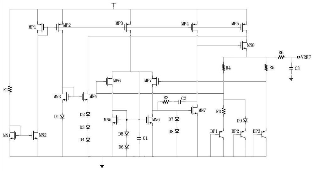
[0015] like figure 1 As shown, this embodiment provides an anti-single event effect radiation-hardened bandgap reference circuit, including PMOS transistors MP1-MP7; NMOS transistors MN1-MN8; diodes D1-D9; PNP transistors BP1-BP3; resistors R1-R6; C1 to C3.

[0016] R1, MN1, MN2, MP1, MP2, MN3, MN4, D1-D4 are startup circuits, and provide bias current to the entire bandgap reference circuit. After the circuit is started, the gate terminal voltage of MN3 is V D1 +V THN3 , the gate voltage required for MN4 to turn on is V D1 +V D2 +V D3 +V THN4 ≈3V D1 +V THN3 >V D1 +V THN3 , so the shutdown of MN4 after the startup is completed does not affect the normal operation of the reference circuit. At the same time, D1 can effectively discharge the transient current induced by the single particle incident at the drain terminal of MN3, and improve the anti-SET capability.

[0017] MP3, MP6, MP7, MN5, MN6, D5~D8, C1~C2, R2, MN7, MP4, MP5, MN8 constitute an operational amplifier...


PUM


Abstract

The invention relates to an anti-single event effect radiation hardening band-gap reference circuit, which is characterized in that R1, MN1, MN2, MP1, MP2, MN3, MN4 and D1-D4 are starting circuits and provide bias current for the band-gap reference circuit; the MP3, the MP6, the MP7, the MN5, the MN6, the D5-D8, the C1-C2, the R2, the MN7, the MP4, the MP5 and the MN8 form an operational amplifier, the MP3 and the MP4 mirror the current of the MP1 through a current mirror to provide bias for the operational amplifier, the MP5 also mirror the follow-up reference voltage generation part through the current mirror to provide bias for the follow-up reference voltage generation part, and the input end of the operational amplifier is respectively connected with the emitter of the R3 and the emitter of the BP3 for the grid potential of the MP6 and the MP7; and the R4, the R5, the R3, the BP1-BP3, the D9, the R6 and the C3 form a band-gap reference voltage generating circuit. According to the band-gap reference circuit, through small area and power consumption overhead, good radiation resistance is achieved, the lowest working voltage of the circuit is reduced, the application range of the circuit is widened, and the SET resistance is improved through the technology that diodes and capacitors are additionally arranged at important nodes.

Description

technical field [0001] The invention relates to the technology of anti-radiation hardening integrated circuits, in particular to a reference circuit of anti-single event radiation hardening bandgap. Background technique [0002] A bandgap reference circuit is used to generate a voltage reference with a small temperature dependence. Its theoretical basis is to use the superposition of two voltage signals with opposite temperature coefficients and basically equal absolute values ​​to obtain a voltage with approximately zero temperature coefficient. In the present invention, the negative temperature coefficient voltage is realized by the base-emitter PN junction voltage of the PNP triode; and two PNP tubes operating under different current densities are used, and the difference between their base-emitter voltages constitutes the positive temperature coefficient voltage . [0003] The invention belongs to an analog integrated circuit, and the anti-radiation hardening technolog...

Claims


Application Information

Patent Timeline
IPC IPC(8): G05F1/567
CPCG05F1/567
Inventor 邱旻韡屈柯柯
Owner 58TH RES INST OF CETC
Learn More