
Near-field optical device based on nano antenna enhancement effect and manufacturing method thereof

A near-field optics, enhancement effect technology, applied in nano-optics, nano-technology for sensing, nano-technology, etc., can solve the problems of low signal-to-noise ratio, low sensitivity, etc., achieve good stability, simple manufacturing process, The effect of improving test sensitivity and signal-to-noise ratio

Pending Publication Date: 2022-07-22
HANGZHOU DIANZI UNIV
View PDF0 Cites 0 Cited by
  • Summary
  • Abstract
  • Description
  • Claims
  • Application Information

AI Technical Summary

Problems solved by technology

[0004] Aiming at the problems of low sensitivity and low signal-to-noise ratio when using low-refractive-index organic nanomaterials that characterize molecular layer thickness in the prior art, the present invention discloses a near-field optical device based on nano-antenna enhancement effect and its fabrication In the method, the near-field optical device includes an underlying substrate and a phonon polariton resonance excitation crystal film from bottom to top, and the phonon polariton resonance excitation crystal film is a localized electromagnetic enhancement structure

Method used


Image

  • Near-field optical device based on nano antenna enhancement effect and manufacturing method thereof
  • Near-field optical device based on nano antenna enhancement effect and manufacturing method thereof
  • Near-field optical device based on nano antenna enhancement effect and manufacturing method thereof

Examples


Embodiment Construction

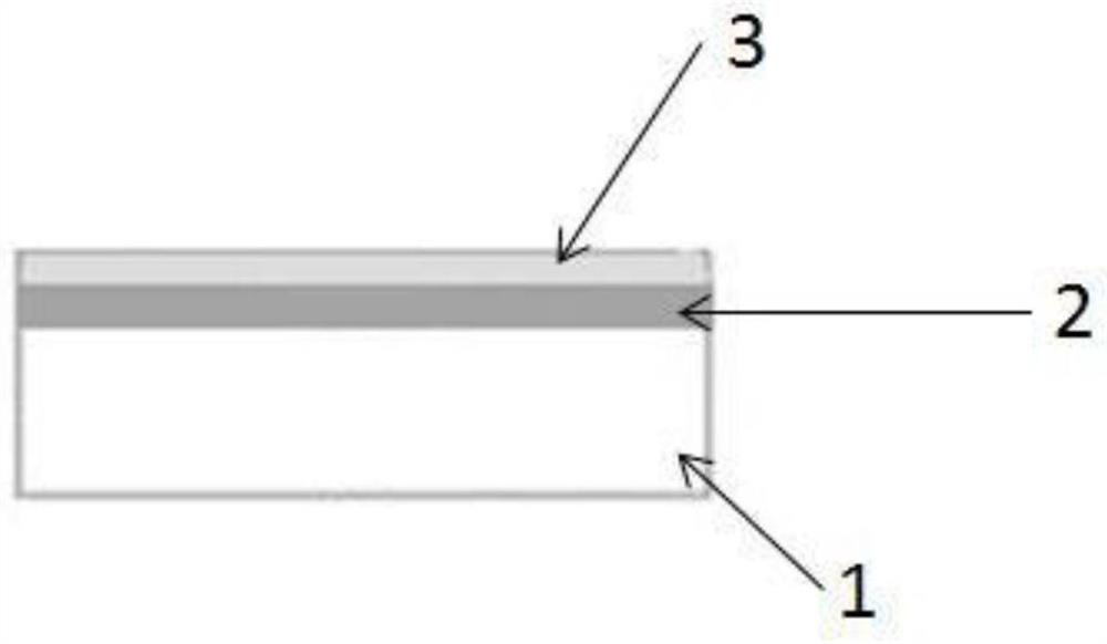
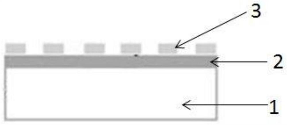
[0036] The near-field optical device based on the nano-antenna enhancement effect in this embodiment, such as Figures 7~9 As shown, the design concept is to construct local electromagnetically enhanced artificial micro-nano structures from the perspective of substrate surface enhancement technology to promote the weak near-field scattering of nano-Fourier transform infrared spectroscopy (nano-FTIR) probes signal to achieve high-sensitivity, super-resolution infrared spectroscopy detection of molecular-level nanomaterials, including a substrate 1 made of clean silicon wafers and a phonon resonance excitation crystal film 2, wherein the phonon resonance excitation crystal film 2 In order to be able to form extremely strong electromagnetic enhancement hot spots, a local electromagnetic enhancement structure is adopted. The phonon resonance excitation crystal film 2 is attached to the upper surface of the substrate 1, the side of the phonon excitation resonance excitation crystal...


PUM

PropertyMeasurementUnit
Thicknessaaaaaaaaaa

Abstract

The invention discloses a near-field optical device based on a nanometer antenna enhancement effect and a manufacturing method of the near-field optical device, and provides the near-field optical device based on the nanometer antenna enhancement effect in order to solve the problems of low sensitivity and low signal-to-noise ratio caused by the adoption of a low-refractive-index organic nanometer material representing the thickness of a molecular layer in the prior art. Comprising a substrate and a phonon excimer resonance excitation crystal film with a local electromagnetic enhancement structure, and further discloses a manufacturing method of the near-field optical device based on the nano-antenna enhancement effect, the manufacturing method comprises the following steps: firstly, depositing the crystal film on the substrate, then spin-coating photoresist on the crystal film, patterning the photoresist, then coating a chromium metal layer on the photoresist, and finally forming the nano-antenna enhancement effect on the chromium metal layer, thereby obtaining the near-field optical device based on the nano-antenna enhancement effect. And finally, stripping the metal layer and the residual adhesive. The manufacturing process is simple and good in stability; the local electromagnetic enhancement structure forms an extremely strong electromagnetic enhancement'hot spot ', can promote weak near-field infrared absorption response of an object to be tested, and improves the test sensitivity and the signal-to-noise ratio of the nanometer Fourier transform infrared spectrum.

Description

technical field [0001] The invention relates to the field of near-field optical detection of nano-antennas, in particular to a near-field optical device based on the enhancement effect of nano-antennas and a manufacturing method thereof. Background technique [0002] Nano Fourier Transform Infrared Spectroscopy is a near-field infrared measurement technology based on atomic force microscope architecture. It combines the advantages of scattering scanning near-field optical microscopy and far-field Fourier transform infrared spectroscopy. Light is irradiated on the tip of the probe, and the coordinated scattering field signal of the probe and the sample is collected, so as to obtain the infrared scattering or absorption spectrum of the local analyte under the tip. Nano Fourier transform infrared spectroscopy can directly test the infrared spectrum of micro-area with 10 nm spatial resolution. It is an important super-resolution method to characterize the infrared properties of ...

Claims


Application Information

Patent Timeline
IPC IPC(8): G01N21/35B82Y15/00B82Y20/00B82Y40/00
CPCG01N21/35B82Y15/00B82Y20/00B82Y40/00G01N2021/3595
Inventor 李闰虎张雪峰胡鑫张鉴刘先国
Owner HANGZHOU DIANZI UNIV
Learn More