Light-emitting auxiliary material and preparation method thereof, light-emitting device and light-emitting device

A technology of auxiliary materials and light-emitting devices, applied in the field of materials, can solve the problems of insignificant improvement of lifespan and luminous efficiency, and achieve the effect of high hole transport efficiency

Pending Publication Date: 2022-07-26
JILIN OPTICAL & ELECTRONICS MATERIALS
View PDF10 Cites 2 Cited by
  • Summary
  • Abstract
  • Description
  • Claims
  • Application Information

AI Technical Summary

Problems solved by technology

[0005] The purpose of this application is to provide a luminescence auxiliary material, which aims to solve the problems that the existing functional materials that can form a luminescence auxiliary layer do not significantly improve the lifespan and luminous efficiency of OLEDs.

Method used


Image

  • Light-emitting auxiliary material and preparation method thereof, light-emitting device and light-emitting device
  • Light-emitting auxiliary material and preparation method thereof, light-emitting device and light-emitting device
  • Light-emitting auxiliary material and preparation method thereof, light-emitting device and light-emitting device

Examples


preparation example Construction

[0060] There is no limitation on the preparation method of the light-emitting device in this application, and conventional methods in the field are sufficient. In this application, methods such as thin film evaporation, electron beam evaporation or physical vapor deposition are preferably used to evaporate metals and conductive oxides on the substrate. and their alloys to form an anode, and then an organic layer and an evaporation cathode are formed thereon to obtain a light-emitting device.

[0061] The light-emitting device provided in this application can be applied to an organic light-emitting device (OLED), an organic solar cell (OSC), an electronic paper (e-paper), an organic photoreceptor (OPC) or an organic thin film transistor (OTFT).
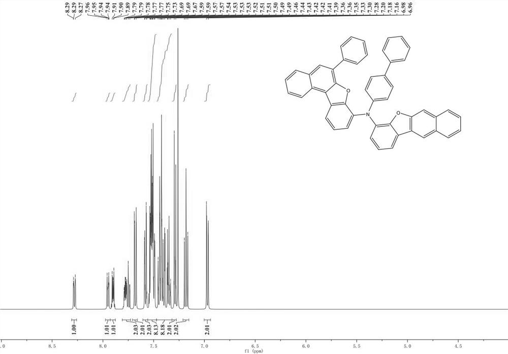
Embodiment 1

[0065]

[0066] After dissolving raw material A-1 (30.00 mmol) and raw material B-1 (30.00 mmol) in toluene, under N 2 Add Pd to the atmosphere 2 (dba) 3 (0.30mmol), P(t-Bu) 3 (1.50 mmol) and t-BuONa (60.00 mmol), heated to 100 °C and stirred for 8 h. After the reaction was completed, use diatomaceous earth to filter while hot to remove salt and catalyst. After the filtrate was cooled to room temperature, distilled water was added to the filtrate. Washing was carried out in , the organic phase was retained after separation, the aqueous phase was extracted with ethyl acetate, and the combined organic layers were then dried using magnesium sulfate, and the solvent was removed using a rotary evaporator. Using a mixed solution of dichloromethane and petroleum ether (V:V=10:4), the remaining material was purified by column chromatography to obtain Intermediate 1 (10.57g, yield: 76.3%);

[0067] After dissolving intermediate 1 (21.67 mmol) and starting material C-I-1 (21.67 mm...
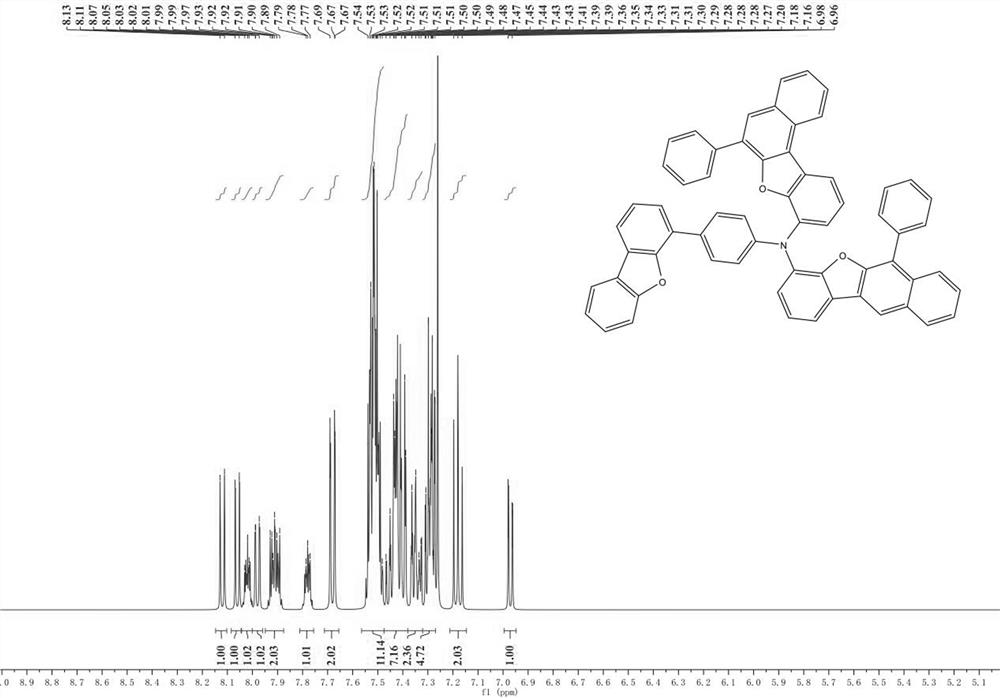
Embodiment 2

[0076]

[0077] After dissolving raw material A-27 (30.00 mmol) and raw material B-27 (30.00 mmol) in toluene, under N 2 Add Pd to the atmosphere 2 (dba) 3 (0.30mmol), P(t-Bu) 3 (1.50 mmol) and t-BuONa (60.00 mmol), heated to 100 °C and stirred for 8 h. After the reaction was completed, use diatomaceous earth to filter while hot to remove salt and catalyst. After the filtrate was cooled to room temperature, distilled water was added to the filtrate. Washing was carried out in , the organic phase was retained after separation, the aqueous phase was extracted with ethyl acetate, and the combined organic layers were then dried using magnesium sulfate, and the solvent was removed using a rotary evaporator. Using a mixed solution of dichloromethane and petroleum ether (V:V=10:4), the remaining material was purified by column chromatography to obtain Intermediate 1 (12.41 g, yield: 75.0%);

[0078] After dissolving intermediate 1 (21.75 mmol) and starting material C-I-27 (21.7...


PUM

PropertyMeasurementUnit
thicknessaaaaaaaaaa

Abstract

The invention is suitable for the technical field of materials, and provides a light-emitting auxiliary material, a preparation method thereof, a light-emitting device and a light-emitting device. Derivative groups of furan and the like are connected to a triarylated amine main body structure, the triarylated amine structure has nitrogen atoms containing lone pair electrons, the electrons on the nitrogen atoms are subjected to transition transfer under the action of an external electric field, molecules generate holes, and reverse transfer of the holes is realized; the triarylamine has good hole transport capability, the furan derivative group is a weak electron-donating group, a geometric structure is added on the basis of a non-planar molecular structure to form a compound with a relatively large spatial configuration, and the unique structure of the compound is beneficial to hole transport, so that relatively high hole transport efficiency is obtained.

Description

technical field [0001] The present application belongs to the technical field of materials, and in particular relates to a light-emitting auxiliary material and a preparation method thereof, a light-emitting device, and a light-emitting device. Background technique [0002] OLED materials are classified into light-emitting materials, hole transport materials, electron transport materials, and the like. Among them, hole transport materials usually have a low highest occupied molecular orbital (HOMO) value. The charge in the light-emitting or light-emitting layer is not balanced, so that light is emitted at the interface of the hole-transporting layer, which reduces the color purity and efficiency of the organic electroluminescent device, and shortens the lifespan. [0003] The hole transport layer (HTL) is responsible for regulating the injection rate and amount of holes. In the OLED, copper phthalocyanine (CuPc), 4,4'-bis[N-(1-naphthyl)-N-benzene Amino] biphenyl (NPB), N,N...

Claims


Application Information

Patent Timeline
Patent Type & Authority Applications(China)
IPC IPC(8): C07D307/77C07D307/91C07D405/14C07D409/14H01L51/54H01L51/50
CPCC07D307/77C07D307/91C07D409/14C07D405/14H10K85/636H10K85/626H10K85/615H10K85/6576H10K85/6574H10K85/6572H10K50/156
Inventor 汪康马晓宇王永光金成寿黄悦张思铭
Owner JILIN OPTICAL & ELECTRONICS MATERIALS
Why Eureka
Try Eureka