Graphene film and transfer method thereof
A technology of graphene film and transfer method, which is applied in the direction of graphene, chemical instruments and methods, nano-carbon, etc., can solve problems such as poor cleanliness, graphene film wrinkle density that cannot meet flexible devices, and restricts the excellent performance of graphene film. , to achieve the effect of improving the cleanliness
- Summary
- Abstract
- Description
- Claims
- Application Information
AI Technical Summary
Problems solved by technology
Method used
Image

Examples
Embodiment 1
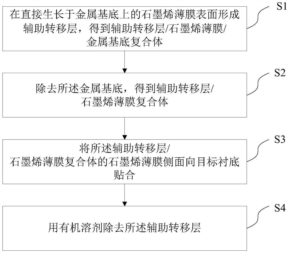
[0036] A single-layer graphene film grown on a 5cm×5cm copper substrate was selected. Dissolve PPC (molecular weight 50000) in anisole, the mass content of PPC is 10%, place the copper foil / graphene film in a glue dispenser, spin-coat the PPC solution on graphite at 1000r / min rotation speed The surface of the graphene film was cured at 60°C for 90s to obtain a PPC layer / graphene film / copper substrate composite, wherein the thickness of the PPC layer was 2 μm. Immerse the PPC layer / graphene film / copper substrate composite in a sodium persulfate etching solution, and after the metal foil is completely etched, use a glass sheet to pick up the PPC layer / graphene film floating in the etching solution , put into deionized water, soak for 15 minutes, repeat once. The PPC layer / graphene film was picked up using the target substrate (sapphire double-polishing sheet), and after natural drying, the PPC layer / graphene film / target substrate was immersed in acetone vapor for 7 minutes to r...
Embodiment 2
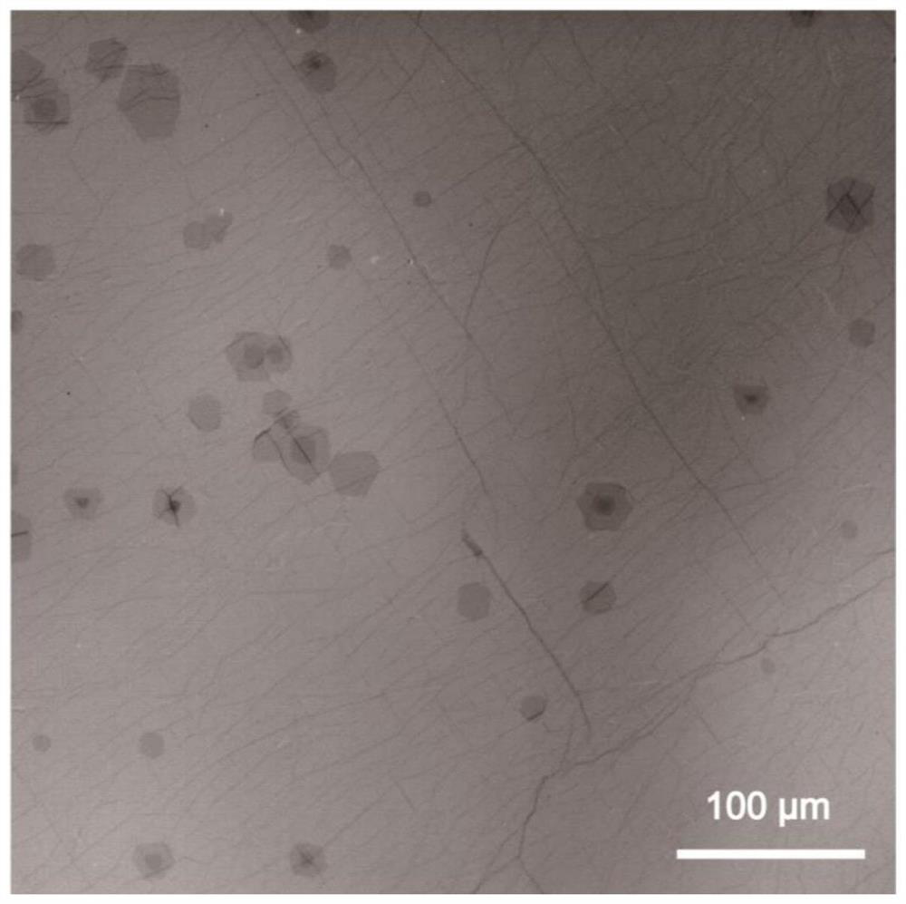
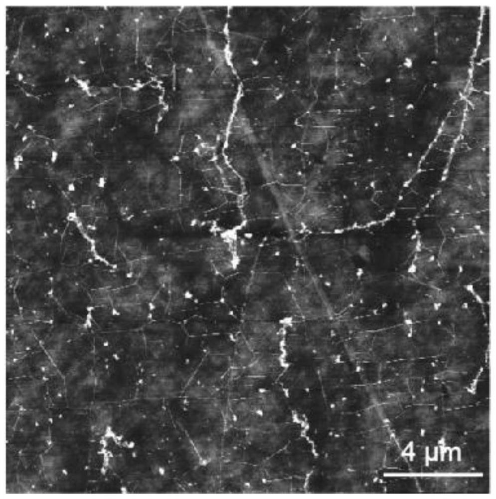
[0039] Except the target substrate is SiO 2 / Si substrate and polymer are selected PCL (molecular weight 45000), other methods are the same as in Example 1, the graphene film can also be successfully transferred to SiO 2 / Si substrate. PCL was dissolved in ethyl lactate, and the mass content of PCL was 10%. like Figure 4 shown, transfer to SiO 2 The graphene film on the / Si substrate is complete and uniform. Observe the Raman spectrum of the graphene film after transfer, as Figure 5 shown, transfer to SiO 2 The graphene films on / Si substrates conform to the typical Raman spectroscopic characterization of single-layer graphene.
Embodiment 3
[0041] Except using 10cm×30cm copper foil as the substrate to produce the graphene film and using PET as the substrate, other steps and conditions are the same as in Example 1, and the graphene film is transferred to the PET substrate. After observation, it was found that the transferred graphene film had good cleanliness, good integrity and no damage.
PUM
 Abstract
Description
Claims
Application Information
 - R&D
- Intellectual Property
- Life Sciences
- Materials
- Tech Scout
- Unparalleled Data Quality
- Higher Quality Content
- 60% Fewer Hallucinations
Browse by: Latest US Patents, China's latest patents, Technical Efficacy Thesaurus, Application Domain, Technology Topic, Popular Technical Reports.
© 2025 PatSnap. All rights reserved.Legal|Privacy policy|Modern Slavery Act Transparency Statement|Sitemap|About US| Contact US: help@patsnap.com