
Surface biocompatibility modification method of semiconductor nanocrystal

A biocompatibility and semiconductor technology, applied in the direction of nanotechnology, nanotechnology, chemical instruments and methods, etc., can solve the problems of poor stability of nanoparticles in water phase, cumbersome processing steps, large consumption of organic solvents, etc., and achieve low cost, Low-cost, environment-friendly effect

Pending Publication Date: 2022-07-29
INST OF CHEM CHINESE ACAD OF SCI
View PDF10 Cites 0 Cited by
  • Summary
  • Abstract
  • Description
  • Claims
  • Application Information

AI Technical Summary

Problems solved by technology

[0005] The technical problem to be solved in the present invention is to provide an environmentally friendly, efficient and clean, non-toxic ligand replacement method that can maintain the fluorescence performance of semiconductor nanocrystals, so as to overcome the cumbersome post-processing steps of the existing ligand replacement, consume a large amount of organic solvents, Defects such as poor stability of the obtained aqueous phase nanoparticles

Method used

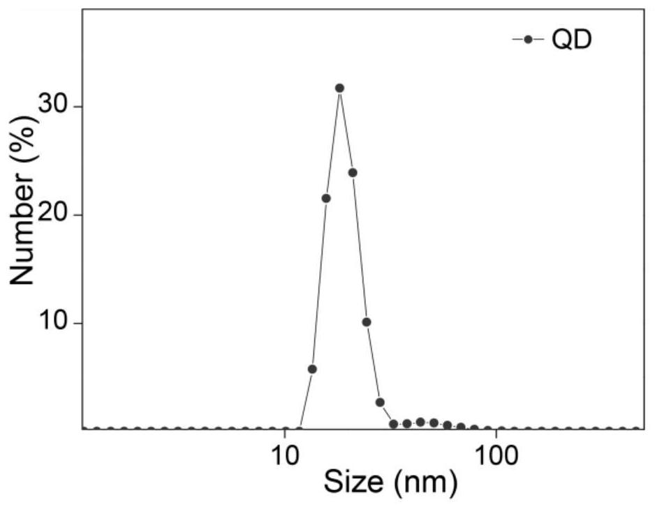
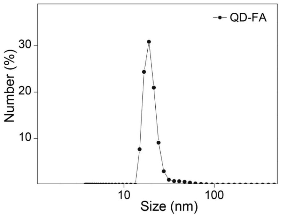
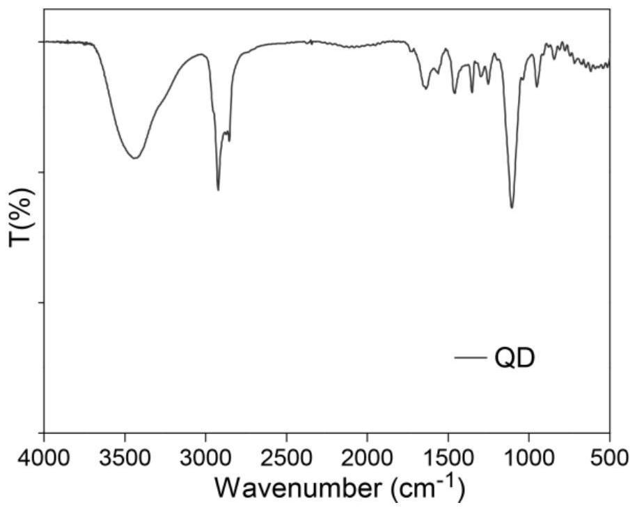

Image

  • Surface biocompatibility modification method of semiconductor nanocrystal
  • Surface biocompatibility modification method of semiconductor nanocrystal
  • Surface biocompatibility modification method of semiconductor nanocrystal

Examples


Embodiment 1

[0071] Preparation of water-soluble semiconductor nanocrystals by ligand replacement reaction: PEG molecules (PEG molecular weight: 1000) with a thiol group at one end and a methoxy group at the other end were selected as ligands, and 10 mg of dodecyl thiol ligand-modified CuInS 2 The @ZnS semiconductor nanocrystals were dispersed in 5 mL of ethyl acetate, and then added to 10 mL of ethyl acetate solution containing 200 mg of ligands. The mixed solution was heated to 55 °C and stirred with nitrogen for 5 h, and then extracted with water to obtain PEG-modified Aqueous quantum dots were purified by dialysis or ultrafiltration to remove free ligands, and finally dispersed in ultrapure water and stored in a refrigerator at 4°C for further use.

Embodiment 2

[0073] Preparation of water-soluble semiconductor nanocrystals by ligand replacement reaction: PEG molecules (PEG molecular weight: 2000) with a thiol group at one end and a methoxy group at the other end were selected as ligands, and 10 mg of dodecyl mercaptan, oleic acid, oleylamine Ligand co-modified CuInSe 2 @ZnS was dispersed in 5 mL of toluene, and then added to 10 mL of toluene solution containing 200 mg of ligands. The mixed solution was heated to 80 °C and stirred with nitrogen for 5 h, and then extracted with water to obtain PEG-modified aqueous quantum dots. The free ligands were removed by ultrafiltration and finally dispersed in ultrapure water and stored in a refrigerator at 4°C for further use.

Embodiment 3

[0075] Preparation of water-soluble semiconductor nanocrystals by ligand replacement reaction: PEG molecules (PEG molecular weight: 2000) with a thiol group at one end and a methoxy group at the other end were selected as ligands, and 10 mg of dodecyl thiol ligand-modified CuInSe 2 @ZnS was dispersed in 5 mL of ethyl acetate, then added to 20 mL of ethyl acetate solution containing 50 mg of ligand, the mixed solution was heated to 50 °C and stirred with nitrogen for 5 h, and then extracted with water to obtain PEG-modified aqueous quantum At this point, the free ligands were removed by dialysis or ultrafiltration purification, and finally dispersed in ultrapure water and stored in a refrigerator at 4°C for further use.


PUM


Abstract

The invention discloses a ligand replacement method which is environment-friendly, efficient, clean, non-toxic, simple in step, low in cost and capable of keeping the fluorescence property of semiconductor nanocrystals. Functionalized biocompatible ligand molecules are adopted to replace hydrophobic ligand molecules on the original surface of the semiconductor nanocrystal, and the water-soluble (water-dispersible) and surface biocompatible modified semiconductor nanocrystal is obtained. The method overcomes the defects that the existing ligand replacement post-treatment steps are tedious, a large amount of organic solvents and precipitants are consumed, and the stability of the obtained water-phase nanoparticles is poor. And the types and the number of the ligands on the surface of the nanocrystal are accurately controlled by changing feeding, so that the semiconductor nanocrystal which is stably dispersed in water and a physiological buffer solution and of which the surface can be modified with biological functional molecules is finally obtained. The surface of the water-soluble semiconductor nanocrystal is chemically modified, so that the water-soluble semiconductor nanocrystal becomes a biological functionalized nanocrystal, and the biological functionalized nanocrystal can be used as a nanoprobe for in-vivo and in-vitro biological detection and disease treatment.

Description

technical field [0001] The invention relates to a method for ligand replacement and biocompatibility modification on the surface of a semiconductor nanocrystalline material, and belongs to the technical field of nanomaterial surface interface engineering. Background technique [0002] Nanomaterials refer to materials with at least one dimension in the nanometer size range (1-100 nm) in three-dimensional space, and materials constructed with them as units. In the past three decades, nanomaterials, especially functional nanomaterials with various special physical and chemical properties (optical, magnetic, electrical, catalysis and adsorption, etc.) endowed by size effects and surface effects, have been proved in biology, medicine. It has a wide range of applications in other fields, including in vitro diagnosis, in vivo imaging, nanomedicine and therapy. Quantum dots, also known as semiconductor nanocrystals, are nanoparticles composed of II-VI, II-V, III-V, IV-VI, I-VI, I-I...

Claims


Application Information

Patent Timeline
Patent Type & Authority Applications(China)
IPC IPC(8): C09K11/02C09K11/62C09K11/88A61K49/00B82Y30/00B82Y40/00
CPCC09K11/02C09K11/025C09K11/623C09K11/883A61K49/0019A61K49/0052B82Y30/00B82Y40/00
Inventor 荆莉红李颖颖高明远
Owner INST OF CHEM CHINESE ACAD OF SCI
Learn More