Focusing type vertical grating coupler and preparation method thereof
A vertical grating and focusing grating technology, applied in the direction of instruments, light guides, optics, etc., can solve the problems of small coupling tolerance and low coupling efficiency, and achieve the effect of enhancing interference, improving coupling efficiency, and increasing coupling light source
- Summary
- Abstract
- Description
- Claims
- Application Information
AI Technical Summary
Problems solved by technology
Method used
Image
Examples
Embodiment 1
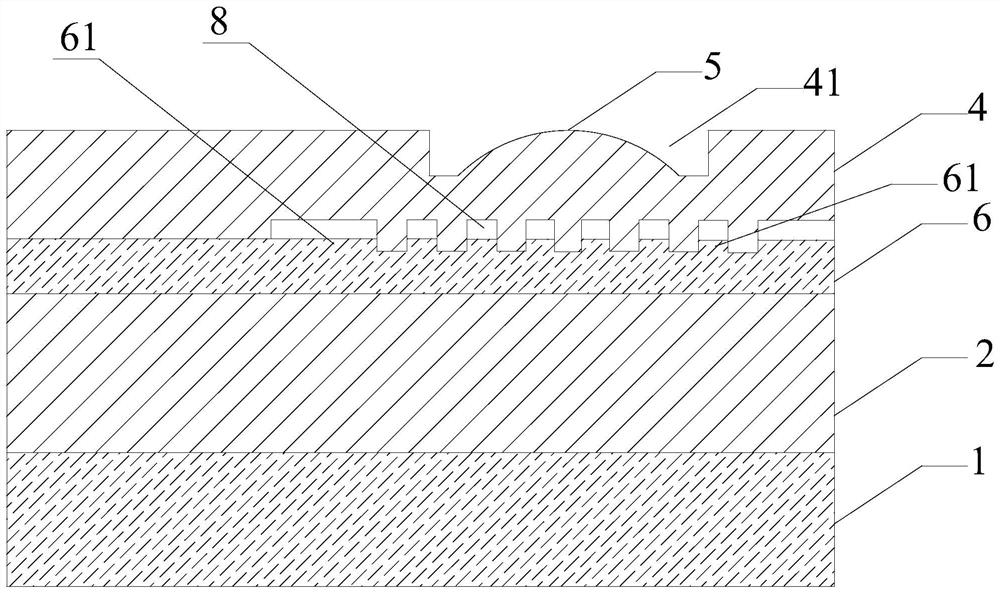
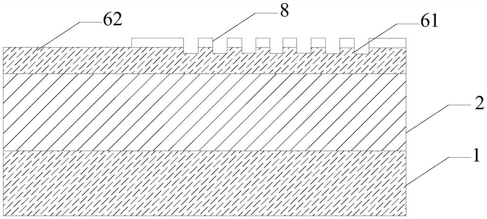
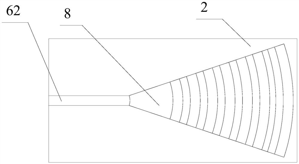
[0029] Example 1: as Figure 1 to Figure 4 As shown, this embodiment provides a focusing vertical grating coupler, which is manufactured based on an SOI substrate, and the SOI substrate sequentially includes a silicon substrate layer 1 , a silicon dioxide buried oxide layer 2 and a top silicon layer 3 from bottom to top , a top silicon waveguide layer 6 is etched on the top silicon layer 3, and the top silicon waveguide layer 6 is composed of a fan-shaped focusing grating waveguide structure 61 and a strip-shaped waveguide structure 62 connected to the fan-shaped focusing grating waveguide structure 61. The focusing grating waveguide structure 61 is covered with a polysilicon layer 8, the polysilicon layer 8 and the top silicon waveguide layer 6 around it are covered with a silicon dioxide cladding layer 4, and the top of the silicon dioxide cladding layer 4 is provided with a fan-shaped focusing grating waveguide. The position of the structure 61 corresponds to the focusing c...
Embodiment 2
[0036] Example 2: as Figure 5 As shown, this embodiment provides a preparation method of the focusing vertical grating coupler, which is characterized by comprising the following steps:
[0037] step 1, Figure 5 As shown in a, prepare the SOI substrate, and clean the top silicon layer 3;
[0038] Step 2. Figure 5 As shown in b, polysilicon is deposited on the top silicon layer 3 to form a polysilicon layer 8;
[0039] Step 3. Figure 5 As shown in c, the photoresist 7 is uniformly coated on the polysilicon layer 8;
[0040] Step 3. Figure 5As shown in d, according to the size and shape of the fan-shaped focusing grating waveguide structure 61 and the strip-shaped waveguide structure 62, the photoresist 7 is exposed by the laser direct writing 3D grayscale lithography technology, and then developed to obtain the photoresist layer focusing Grating waveguide structure pattern 9;
[0041] Step 4. Figure 5 As shown in e, by reactive ion etching, the photoresist layer f...
PUM
| Property | Measurement | Unit |
|---|---|---|
| Etching depth | aaaaa | aaaaa |
| Length | aaaaa | aaaaa |
| Width | aaaaa | aaaaa |
Abstract
Description
Claims
Application Information


