Heterojunction solar cell with composite electrode layer and preparation method thereof
A technology of solar cells and composite electrodes, applied in circuits, electrical components, photovoltaic power generation, etc., can solve problems affecting battery performance, complex methods, poor conductivity of silicon-containing films, etc., to achieve reduced ITO film thickness, good reflection, Voc no drop effect
- Summary
- Abstract
- Description
- Claims
- Application Information
AI Technical Summary
Problems solved by technology
Method used
Image
Examples
specific Embodiment approach
[0040] In this embodiment, a composite electrode layer including a TCO layer, a metal film layer and a silicon-containing thin film layer is developed on the back to replace the original single-layer ITO layer, so as to achieve or exceed the performance improvement efficiency of the original single-layer ITO material, and can greatly reduce the The low indium heterojunction cell was successfully fabricated at low cost. The specific implementation is as follows:
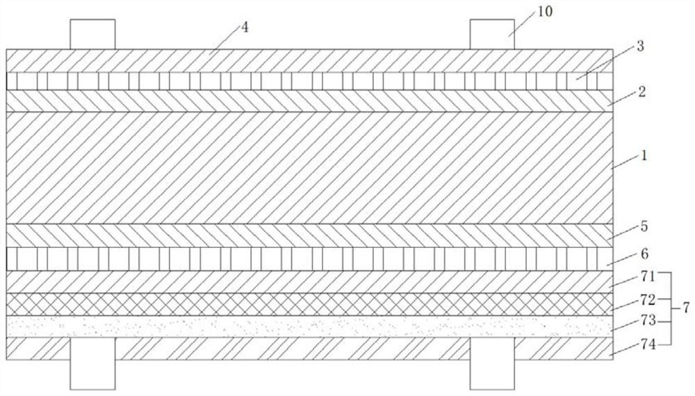
[0041] like figure 1 As shown, the heterojunction solar cell with a composite electrode layer includes using n-type or p-type single crystal silicon c-Si as a substrate 1, and sequentially depositing a first intrinsic amorphous silicon layer 2 (a) on the upper surface of the substrate 1 -SiH(i)), n-type amorphous silicon layer 3 and upper electrode layer 4; sequentially deposit a second intrinsic amorphous silicon layer 5 (a-SiH(i)), p-type amorphous silicon layer on the lower surface of substrate 1 The silicon laye...
Embodiment approach
[0048] As a preferred embodiment, the overall thickness of the lower electrode layer is greater than or equal to 40 nm.
[0049] This embodiment also provides a method for preparing the above-mentioned heterojunction solar cell with a composite electrode layer, comprising the following steps:
[0050] Step 1, the n-type or p-type single crystal silicon wafer is textured to obtain the desired texture;
[0051] Step 2, depositing an intrinsic amorphous silicon layer and an n-type amorphous silicon layer on the upper surface, and depositing an intrinsic amorphous silicon layer and a p-type amorphous silicon layer on the lower surface;
[0052] Step 3: Use magnetron sputtering to deposit a layer of Front ITO with a thickness of 60-90 nm on the upper surface from top to bottom, and use magnetron sputtering or reactive plasma method to deposit a layer of thickness on the lower surface from bottom to top. The RearITO layer is 1-40nm, the AZO layer is 0-90nm thick, the metal film lay...
Embodiment 1
[0060] A preparation method of a heterojunction solar cell with a composite electrode layer, comprising the steps of:
[0061] Step 1, the n-type single crystal silicon wafer is textured to obtain the desired texture;
[0062] Step 2, depositing an intrinsic amorphous silicon layer and an n-type amorphous silicon layer on the upper surface, and depositing an intrinsic amorphous silicon layer and a p-type amorphous silicon layer on the lower surface;
[0063] Step 3: Introduce argon and oxygen at room temperature, set the gas flow ratio of argon to oxygen at 40:1, keep the cavity pressure at 0.5Pa, turn on the sputtering power supply, and use the magnetron sputtering method from the top. On the other hand, a Front ITO layer with a thickness of 75nm is deposited on the upper surface, the power density is 5.07kw / m, the square resistance of the Front ITO layer is 65Ω / □, and the substrate temperature is set to 150℃; the gas flow of argon and oxygen The ratio is set to 33:1, the ca...
PUM
| Property | Measurement | Unit |
|---|---|---|
| thickness | aaaaa | aaaaa |
| thickness | aaaaa | aaaaa |
| thickness | aaaaa | aaaaa |
Abstract
Description
Claims
Application Information


