

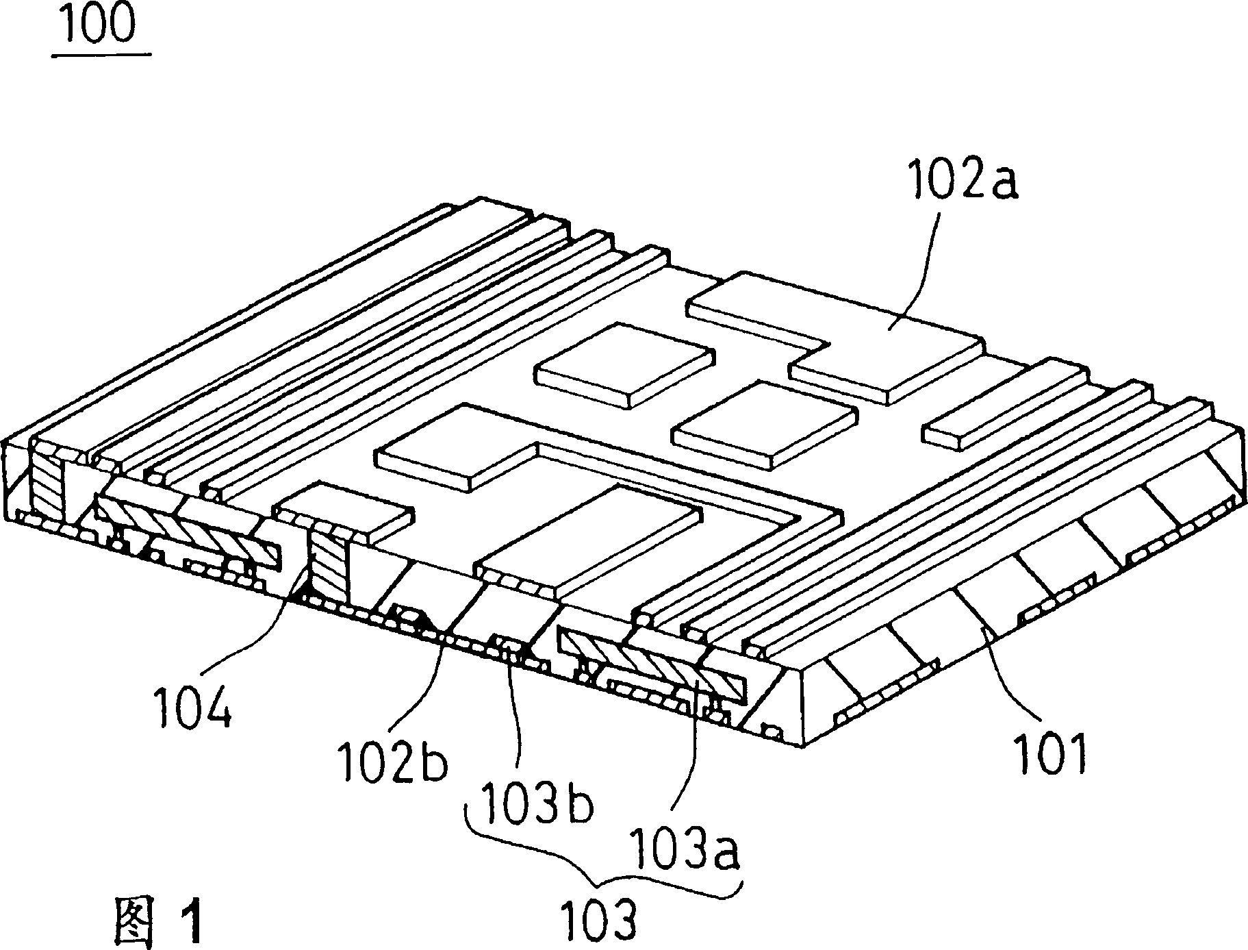
Built-in circuit device assembly and its manufacturing method
A technology of circuit devices and manufacturing methods, which is applied in the fields of printed circuit manufacturing, multilayer circuit manufacturing, semiconductor/solid-state device manufacturing, etc., and can solve the problems of reduced reliability of built-in circuit device components, low thermal conductivity, and insufficient heat dissipation, etc.
- Summary
- Abstract
- Description
- Claims
- Application Information
AI Technical Summary
Problems solved by technology
Method used
Image

Examples
Embodiment 1
[0123] First, an example of a method for producing an electrically insulating substrate composed of a mixture containing an inorganic filler and a thermosetting resin when producing the circuit device built-in module of the present invention will be described.
[0124] In the present example, an electrically insulating substrate was prepared according to the compounding ratio shown in Table 1. Meanwhile, a comparative example is shown as sample number 1.
[0125] sample
thermosetting resin
other additives
(wt%)
(W / mK)
(ppm / °C)
Dielectric constant
1MHz
Dielectric loss
1MHz(%)
Dielectric strength (AC)
KV / mm
type
Amount (wt%)
type
Amount (wt%)
1
Al 2 o 3
60
liquid epoxy resin
WE-2025
39.8
Kabosobratsuku
(0.2)
0.52
45
3.5
...
Embodiment 2
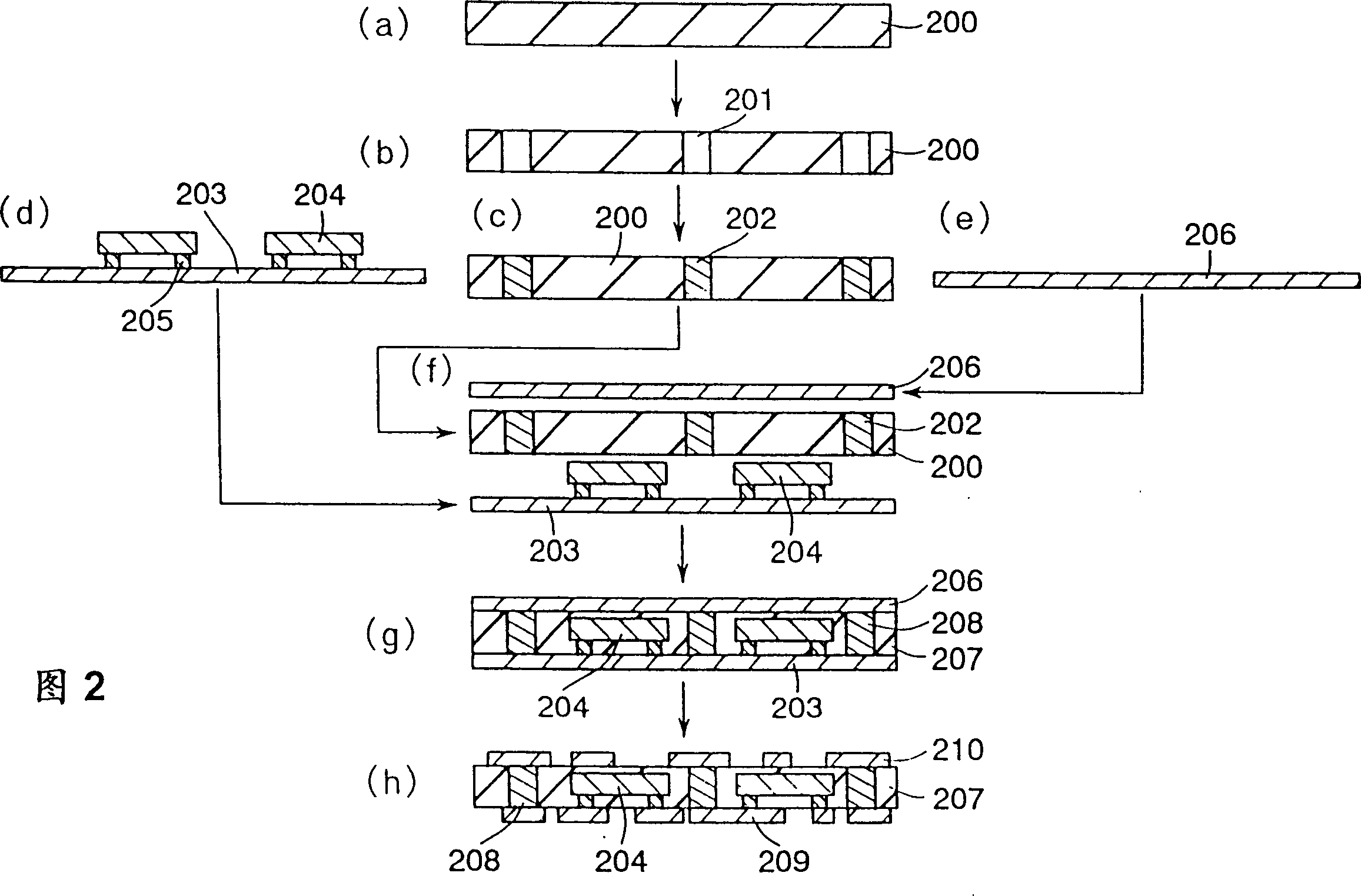
[0146] Embodiment 2 is an example of manufacturing a circuit component built-in module by the method described in Embodiment 2.
[0147] The composition of the electrically insulating substrate used in this example is: 90% by weight of Al 2 o 3 (Showa Denko Co., Ltd., AS-40, spherical shape, average particle diameter 12 μm), 9.5% by weight of liquid epoxy resin (Nippon Recco (Co., Ltd.) product, EF-450), 0.2% by weight of carbon black ( Toyo Ka-bon Co., Ltd.), 0.3% by weight of coupling agent (Ajinomoto Co., Ltd., titanate type, 46B).
[0148] The above-mentioned material was processed under the same conditions as in Example 1 to produce a plate-like body (thickness: 500 μm). The plate-shaped body was cut into a predetermined size, and a through hole (0.15 mm in diameter) for connecting the inner via hole was formed with a carbon dioxide gas laser (see FIG. 2( b )).
[0149] A conductive resin composition is filled in the through holes by screen printing (see FIG. 2( c )). ...
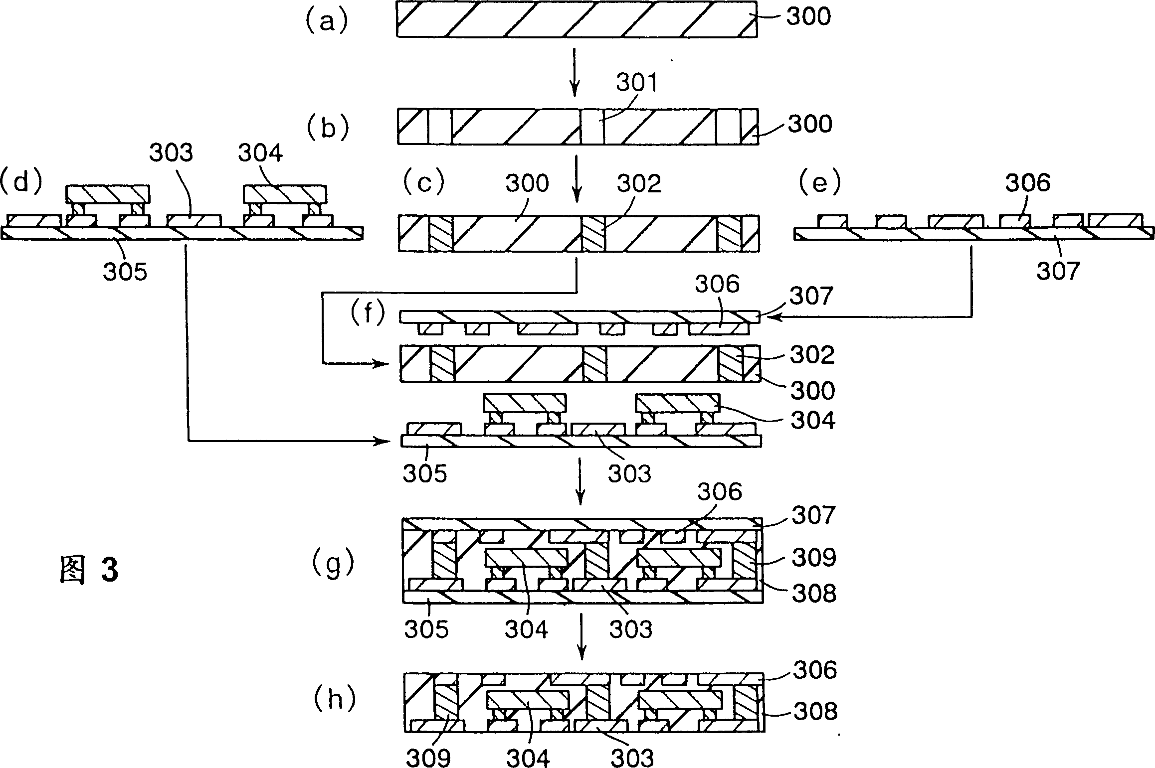
Embodiment 3
[0158] Embodiment 3 is an example of manufacturing a circuit component built-in module by the method described in Embodiment 3.
[0159] First, in the same manner as in Example 2, a plate-like body (500 μm in thickness) in which the through-holes were filled with the conductive resin composition was fabricated (see FIG. 3( c )).
[0160] Then, a copper foil having a thickness of 35 μm was adhered to a release film (made of polyphenylene sulfide, 150 μm thick) with an adhesive. This copper foil is roughened on one side, and the glossy side is the adhesive side at the time of bonding.
[0161] Next, the copper foil on the release film is etched through a photolithography process and an etching process to form a wiring pattern. Further, a semiconductor device is mounted on the wiring pattern by flip-chip bonding using solder bumps (see FIG. 3( d )).
[0162] Next, a sealing resin is injected into the gap between the semiconductor device mounted on the wiring pattern and the wir...
PUM
 Abstract
Description
Claims
Application Information