Lead frame for semiconductor device

A lead frame and semiconductor technology, used in semiconductor devices, semiconductor/solid-state device components, electric solid-state devices, etc., can solve problems such as damage to appearance, inability to meet corrosion resistance, moisture resistance, and impracticality of lead frames. Appearance, good appearance, effect to ensure snug fit

Inactive Publication Date: 2005-02-23
SHINKO ELECTRIC IND CO LTD
View PDF1 Cites 4 Cited by
  • Summary
  • Abstract
  • Description
  • Claims
  • Application Information

AI Technical Summary

Problems solved by technology

During this removal, if the copper-zinc alloy plating film remains on the surface of the material, uneven spots will occur on the tin plating film, which will damage the appearance and reduce the adhesion of the tin plating film
[0012] (4) If there is highly corrosive zinc on the surface of the outer lead part that has not been plated with precious metals, the corrosion resistance and moisture resistance cannot be satisfied, and the surface will deteriorate before the assembly process of the semiconductor device on which the semiconductor chip is mounted. The problem of impracticality of writing as a lead frame

Method used


Image

  • Lead frame for semiconductor device
  • Lead frame for semiconductor device
  • Lead frame for semiconductor device

Examples


specific Embodiment approach

[0070] Hereinafter, preferred embodiments of the present invention will be described with reference to the drawings.

[0071] [plan 1]

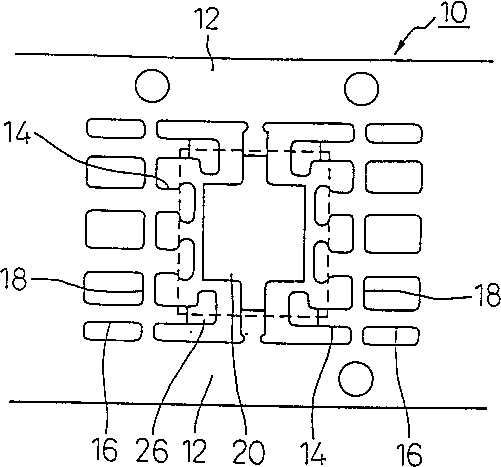
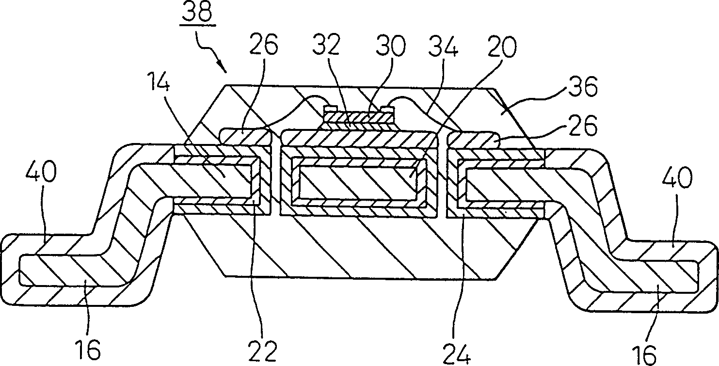
[0072] According to the first invention, such as figure 1 and figure 2 As shown, the copper-based material 8 is stamped or etched to form a lead frame body 10 having a frame 12, an inner lead 14, an outer lead 16, a tie-bar 18, and a chip pad 20. The copper-based material can be Various materials such as pure copper, copper-tin alloy, copper-zinc alloy, copper-iron alloy, and copper-chrome alloy are used.

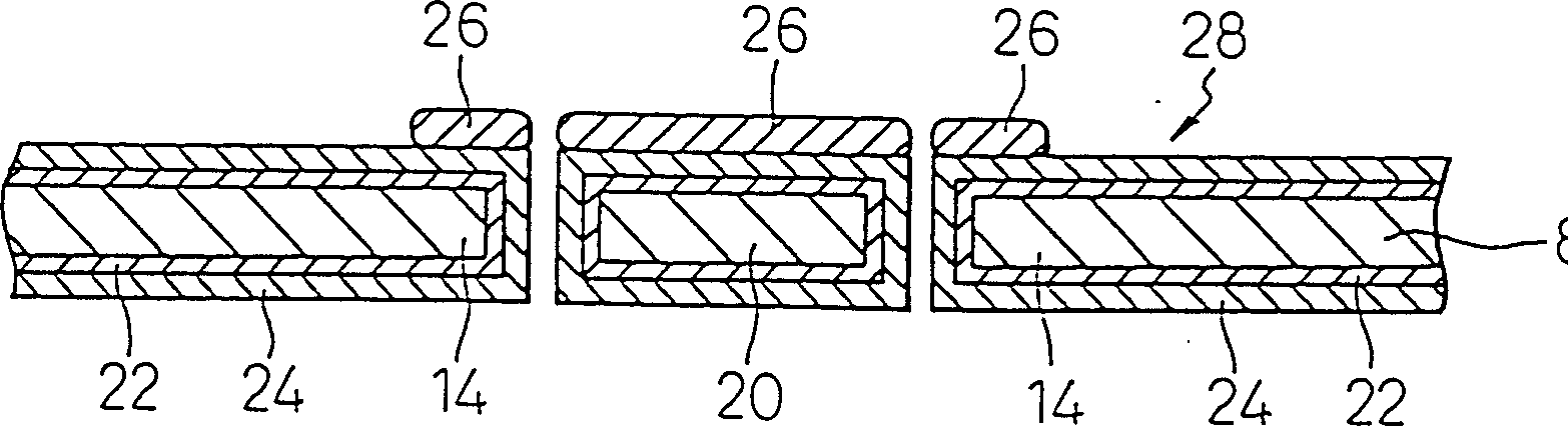
[0073] Next, the galvanized film 22 is formed on the entire surface of the lead frame body 10 . The thickness of the galvanized film 22 is formed to be about 0.001 to 0.5 micron, preferably a strike plating film of about 0.01 micron.

[0074] Next, a copper-plated film 24 having a thickness of 0.02 to 0.4 microns is formed on the zinc-plated film 22 . The thickness of the copper plating film 24 is more preferably 0.1 to 0.3 microns. ...

Embodiment 1、2、3

[0093] On the copper alloy material (Cu-1 ~ 3wt% Sn alloy. The same below), use the above electroplating solution to form a 0.01 micron galvanized film, and use the above electroplating solution to form a thickness of 0.1 micron, 0.3 micron, 0.4 micron on the galvanized film. Micron copper plating film.

[0094] [Scenario 2]

[0095] According to the first invention, the copper-zinc alloy plating film 22 is formed on the lead frame body 10 instead of the zinc plating film 22 . The copper-zinc plating film is also formed to a thickness of about 0.001 to 0.5 micron, and it is desirable to form a strike plating film of about 0.01 micron.

[0096] The composition of the copper-zinc electroplating film is: the ratio of copper is 10-90wt%, and the rest is zinc.

[0097] Next, a copper plating film 24 is formed on the copper-zinc alloy plating film 22 . The thickness of the copper plating film 24 is 0.02 to 0.4 microns, preferably 0.1 to 0.3 microns to strike the plating film. Adhe...

Embodiment 4、5、6

[0109] On the copper alloy material, form a 0.01 micron copper-zinc (copper 50-zinc 50) alloy electroplating film with the above-mentioned electroplating solution, and use the above-mentioned electroplating solution on the copper-zinc alloy electroplating film to form a thickness of 0.1 micron, 0.3 micron, 0.4 micron copper plating film.


PUM

PropertyMeasurementUnit
thicknessaaaaaaaaaa
thicknessaaaaaaaaaa
thicknessaaaaaaaaaa

Abstract

A semiconductor device lead frame made of copper or a copper alloy used for a resin sealing type semiconductor device, comprising a lead frame body made of copper or a copper alloy, a double-layer under plating film formed on the lead frame body and comprising a lower layer made of zinc or a copper-zinc alloy and an upper layer made of copper having a thickness of 0.02 to 0.4 mu m and a precious metal plating film formed on at least a wire bonding portion of an inner lead of the copper upper layer of the under plating film. This lead frame is excellent in adhesion with a sealing resin, is free from contaminate a precious metal plating solution (particularly a silver plating solution), has a good appearance of the precious metal plating film, is excellent in corrosion resistance and moisture resistance, and has a good appearance and adhesion of an external solder plating film.

Description

technical field [0001] The present invention relates to a lead frame for a semiconductor device, a manufacturing method thereof, a semiconductor device using the lead frame, and a manufacturing method thereof. Background technique [0002] In the lead frame for semiconductor devices used in resin-sealed semiconductor devices, copper or copper alloys other than iron-nickel alloys (typically Fe-42%Ni alloys) can be used. Department of material. [0003] In the case of a lead frame using this copper-based material, copper strike plating is generally formed on the surface of the material in order to smoothen the surface and to improve the adhesion of a precious metal plating film such as silver to be formed later. After the film, the above-mentioned noble metal plating film for improving the chip adhesion and wire bonding is formed on the die pad and the wire bonding portion of the inner lead. [0004] In the case of using a copper-based material, a copper oxide film is likely...

Claims


Application Information

Patent Timeline
Patent Type & Authority Patents(China)
IPC IPC(8): H01L23/495
CPCH01L2924/01015H01L2924/01023H01L2924/01046H01L2924/0105H01L2924/01082H01L2924/00014H01L2924/01045H01L2224/32245H01L2924/01019H01L2924/01327H01L2924/01029H01L23/49582H01L2924/01028H01L2224/85439H01L2224/48091H01L2924/014H01L24/48H01L2924/01024H01L2224/484H01L2924/0103H01L24/45H01L2924/01047H01L2924/01079H01L2224/48247H01L2224/45099H01L2924/01033H01L2924/01005H01L2924/01006H01L2224/85464H01L2924/01078H01L2224/05599H01L2224/85444H01L2224/73265H01L2924/181Y10T29/4922Y10T29/49172H01L2924/00012H01L23/50H01L2924/00
Inventor 关和光吉江崇佐藤晴信
Owner SHINKO ELECTRIC IND CO LTD
Why Eureka
Try Eureka