Electroluminescence device and manufacturing method thereof
An electroluminescent display and device technology, applied in the field of electronic devices and manufacturing these devices, can solve problems such as increased production cost and complicated manufacturing process.
- Summary
- Abstract
- Description
- Claims
- Application Information
AI Technical Summary
Problems solved by technology
Method used
Image

Examples
Embodiment 1
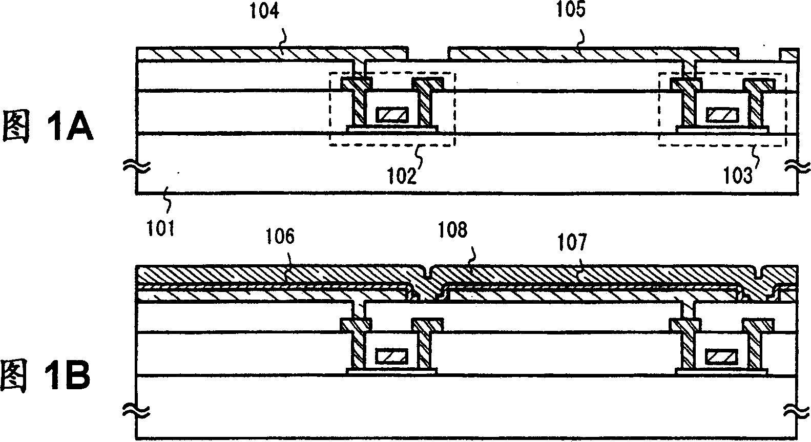
[0027] Embodiments of the present invention are described with reference to FIGS. 1A to 1D . First, TFTs 102, 103 are formed on a substrate 101 by a known method. Although any substrate can be used as the substrate 101, glass substrates, ceramic substrates, plastic substrates, and stainless steel substrates are preferable (FIG. 1A).
[0028] TFT 102, 103 may have any structure. However, since they are both TFTs that control current flowing into the pixel electrodes 104, 105, it is desirable to have a structure that can reduce degradation by heat generation and hot carrier effects. On the other hand, excessive current generates heat to degrade the EL layer, so in some cases, the channel length can be extended or resistors can be placed to suppress excessive current.
[0029] It is to be noted that although FIGS. 1A to 1D illustrate the TFT as if only one TFT is formed in one pixel, in fact, there may be two TFTs, one being a switching TFT and the other being a current control...
Embodiment 2
[0048] This embodiment is described with reference to Figures 2A-2D. First, an auxiliary electrode 202 and a cathode 203 are formed on a substrate 201 . The electrodes and anodes are selectively and successively layered by evaporation and sputtering while using a mask. Although not shown in FIG. 2A, a plurality of electrodes extending in the depth direction at predetermined intervals in the drawing are formed to form a strip.
[0049] The auxiliary electrode 202 is an electrode formed of a material mainly containing aluminum, copper, or silver and having a very low resistivity. In this embodiment, a MgAg alloy is used as the cathode 203, and a low-resistance electrode layered thereon serves as an auxiliary to enhance conductivity, thereby reducing film thickness. Therefore the low resistance electrode is called an auxiliary electrode.
[0050] Then, a light emitting layer 204 is formed so as to cover the auxiliary electrode 202 and the cathode 203 . In this example, Alg 3...
Embodiment 3
[0057] This example describes the case where the impurity element used for doping in Example 1 is changed to another element. The symbols used in Example 1 are cited when necessary.
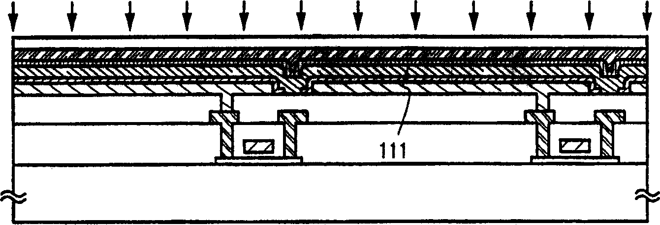
[0058] First, after the steps of Example 1, get Figure 1C status shown. then execute Figure 4 Shown are the impurity element doping steps. In this embodiment, alkali metal elements are doped near the interface between the cathode 107 and the light emitting layer 108, where typical examples include Li (lithium), Na (sodium), K (potassium), Cs (cesium) or alkaline earth metals As an element, typical examples of alkaline earth metal elements include Be (beryllium), Mg (magnesium), Ca (calcium), and Ba (barium). Here, the vicinity of the interface between the cathode and the light-emitting layer means extending 100 nm (usually 50 nm) upward in the depth direction of the light-emitting layer from the interface between the cathode and the light-emitting layer. There is no question of whether the ...
PUM
| Property | Measurement | Unit |
|---|---|---|
| thickness | aaaaa | aaaaa |
| thickness | aaaaa | aaaaa |
Abstract
Description
Claims
Application Information