Production method of millimeter-level microlens array

A technology of microlens array and manufacturing method, which is applied in the directions of lenses, optics, instruments, etc., can solve the problems of components that cannot be processed with arbitrary surface shapes and two-dimensional array structures, difficult to eliminate internal stress, complicated process flow, etc. Reproduce simulation and mold release, controllable vulcanization process, good transparency

Inactive Publication Date: 2005-09-07
INST OF OPTICS & ELECTRONICS - CHINESE ACAD OF SCI
View PDF0 Cites 2 Cited by
  • Summary
  • Abstract
  • Description
  • Claims
  • Application Information

AI Technical Summary

Problems solved by technology

However, this method has the following defects: high thermal expansion coefficient, low softening temperature, strong water absorption, low surface hardness, easy to scratch, difficult to eliminate internal stress, and easy to produce cracks
This method can directly scribe on the surface of optical materials, but it has the following defects: it has strict requirements on the symmetry of the processed components, and generally can only process optical components with linear symmetry and rotational symmetry, and cannot process arbitrary surface shapes and two-dimensional Elements of Array Structure
It can be seen from the replication method disclosed in this article that its technological process is relatively complicated

Method used


Image

  • Production method of millimeter-level microlens array
  • Production method of millimeter-level microlens array
  • Production method of millimeter-level microlens array

Examples


Embodiment 1

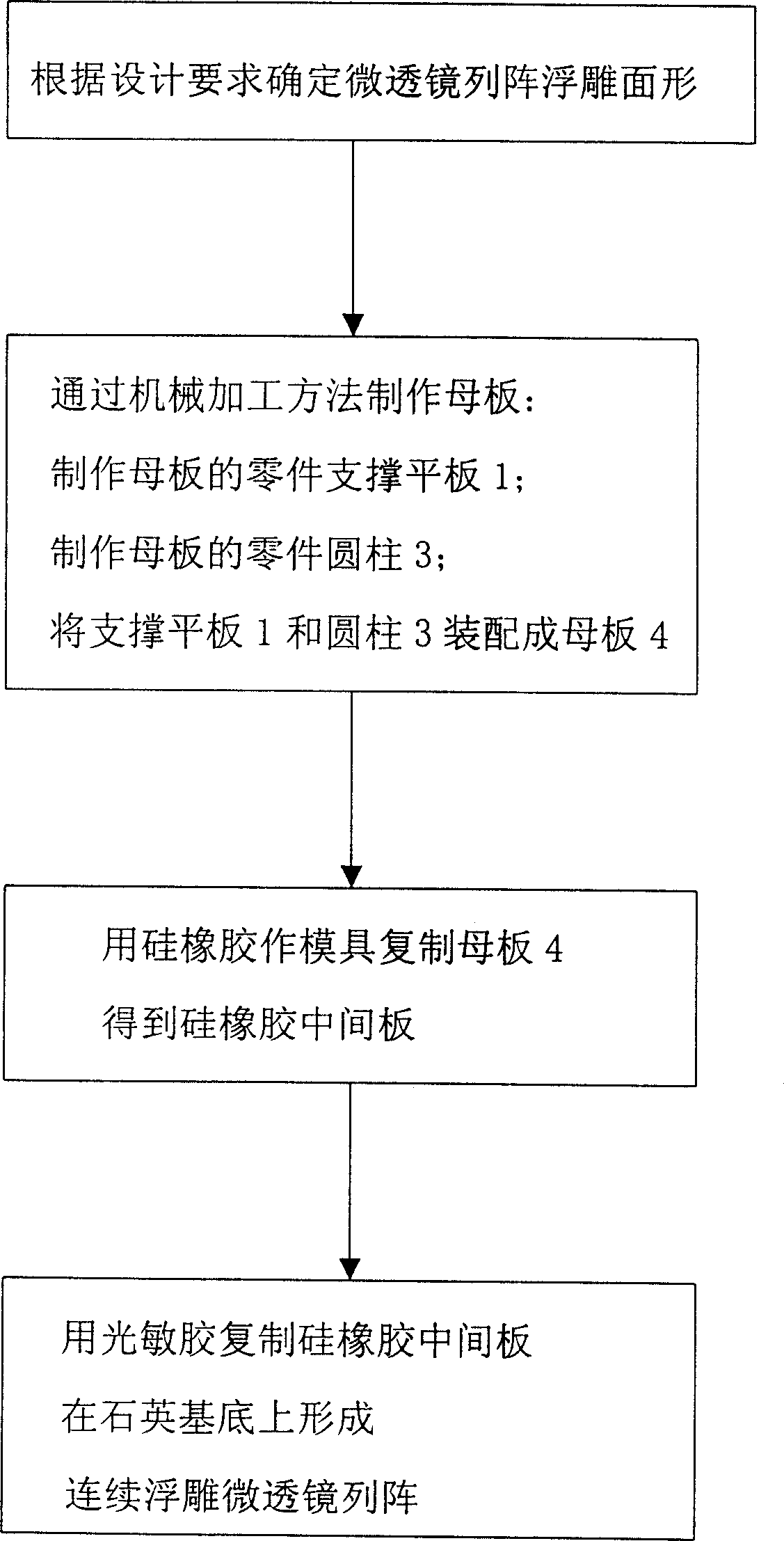
[0039] Embodiment 1 is to manufacture a continuous embossed microlens array with a sub-aperture of φ2 mm, a numerical aperture of 0.2, an array number of 8×8, and a lens sagittal height of 0.2 mm.

[0040] The technological process of embodiment one preparation method is as figure 1 Shown:

[0041] 1, determine microlens embossed surface shape: according to the parameter of embodiment one, the lens that determines the made microlens array is a convex lens, and its curved surface shape is a paraboloid;

[0042] 2. Make the motherboard by machining 4:

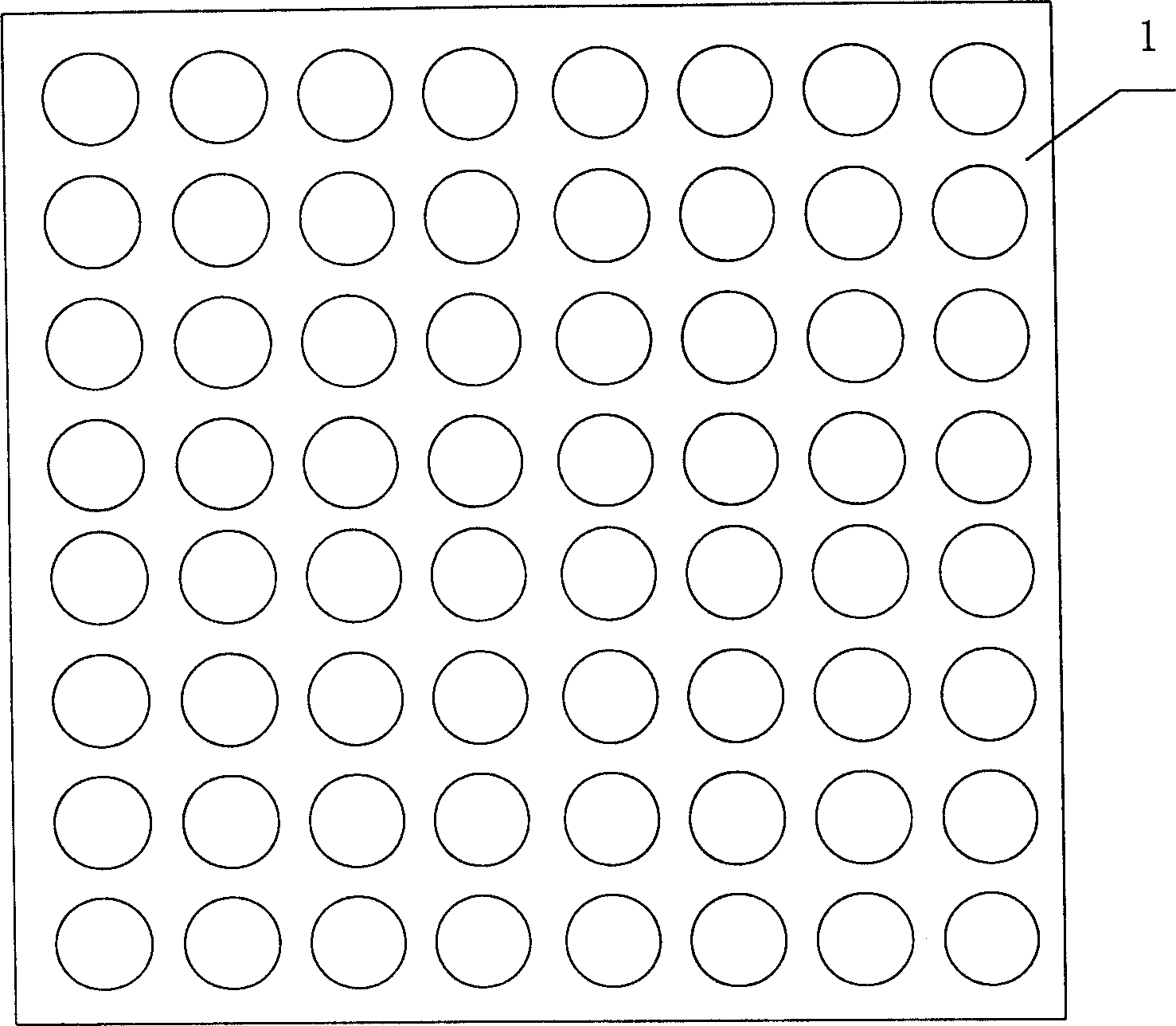
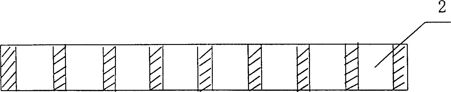
[0043] ①. A supporting plate 1 is made of No. 45 steel. Such as image 3 As shown, a through hole 2 is drilled on the support plate 1, and the diameter of the through hole 2 is equal to the microlens sub-aperture φ2mm. Such as figure 2 As shown, there are 8×8 through holes 2 on the support plate 1, and the distance between the through holes 2 is the center distance of the microlens array;

[0044] ②. Make 8×8 cylinders 3 ....

Embodiment 2

[0048] The second embodiment is to make a continuous embossed microlens array with a sub-aperture diameter of φ3m, an array number of 16×16, and a lens sagittal height of 0.5mm.

[0049] The technological process of embodiment two is as Figure 9 Shown:

[0050] 1. Determine the surface shape of the microlens relief:

[0051] According to embodiment two production parameters, it is determined that the replicated lens is a concave lens, and the curved surface shape is a hyperboloid;

[0052]2. Make the motherboard by mechanical processing:

[0053] According to the determined microlens relief surface shape, the stainless steel is processed by a CNC precision milling machine to make a master plate;

[0054] 3. Copy the master plate with photosensitive adhesive to obtain the microlens relief surface shape required in Embodiment 2, and complete the production of the microlens array.


PUM


Abstract

The present invention discloses a method for making millimeter order microlens array. It is characterized by that it utilizes mechanical treatment to make mother plate of microlens array, then uses the silicon rubber and photosensitizer, etc. to reproduce mother plate, finally, the millimeter order microlens array can be obtained. Because the mechanical treatment possesses higher working accuracy, so that said method can be used for making the millimeter order microlens array with low roughness and good surface form.

Description

technical field [0001] The invention relates to a method for manufacturing a millimeter-scale microlens array. Background technique [0002] The diameter and relief depth of millimeter-scale microlens arrays (diameter from several millimeters to several centimeters, relief depth from hundreds of microns to several millimeters) are between microlens arrays and traditional lenses. Therefore, it is difficult to manufacture millimeter-scale microlens arrays by using the general method for manufacturing microlens arrays, which has defects such as long processing period and complicated process. Using traditional lens processing methods to make millimeter-scale microlens arrays requires processing individual microlenses and then splicing them into microlens arrays. Due to the characteristics of optical processing methods, it is difficult to ensure the consistency of microlenses, which affects Defects in the quality of the microlens array. [0003] In the p...

Claims


Application Information

Patent Timeline
Patent Type & Authority Patents(China)
IPC IPC(8): G02B3/00
Inventor 邓启凌杜春雷
Owner INST OF OPTICS & ELECTRONICS - CHINESE ACAD OF SCI
Why Eureka
Try Eureka