Method for mfg diode

A manufacturing method and diode technology, which are applied in semiconductor/solid-state device manufacturing, electrical components, circuits, etc., can solve the problems of high cost, expensive substrate, and slow diode speed.

Inactive Publication Date: 2006-02-15
SUZHOU GOODARK ELECTRONICS CO LTD
View PDF0 Cites 0 Cited by
  • Summary
  • Abstract
  • Description
  • Claims
  • Application Information

AI Technical Summary

Problems solved by technology

The deficiencies of existing diode manufacturing methods are: 1. The heat treatment temperature is high and consumes a lot of energy. On the one hand, it is not conducive to saving energy. The speed needs to be controlled (heating starts at 850°C at a rate of 10°C / min, and cooling at a rate of 5°C / min from 1200°C to 850°C), so the energy consumption is large
2. After the diode is made, the impurity concentration distribution of the silicon epitaxial wafer changes slowly, see image 3 The distribution state of the diode impurity a) curve, so the diode is slow in operation, the resistance is large, and the power loss is high
3. The thickness of the epitaxial layer of the epitaxial wafer is large (thickness is 8μm), and the substrate is expensive

Method used


Image

  • Method for mfg diode
  • Method for mfg diode
  • Method for mfg diode

Examples


Embodiment 1

[0092] Refer to Table 2 to make a diode under the process conditions.

[0093] The specifications of the epitaxial wafers used are as follows:

[0094] Silicon substrate resistivity 3μΩCM impurity As

[0095] Epitaxial layer resistivity 0.8ΩCM thickness 8μm

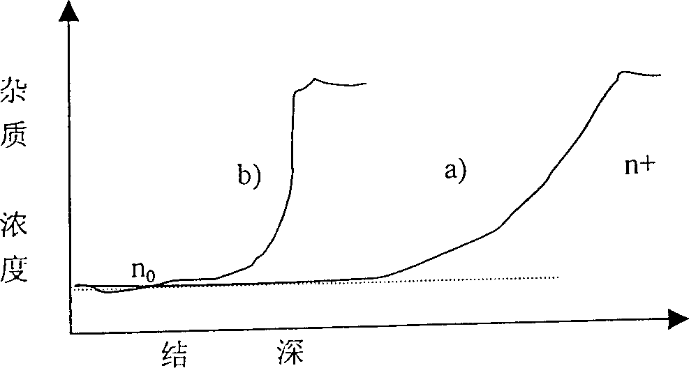
[0096] After making a diode, measure the epitaxial layer thickness and concentration distribution results, see image 3 , b). At this time, the thickness of the epitaxial layer reduced by the steep distribution effect of the impurity layer of the silicon epitaxial layer is 1 μm, that is, the actual thickness of the epitaxial layer is 7 μm. As a result of making a diode, the forward voltage drop of the diode, V f is 0.65V. This is because of the thickness of the actual epitaxial layer.

[0097] The specific process steps are as follows:

[0098] 1. Clean the semiconductor silicon wafer. Ammonium hydroxide (NH 4 OH), hydrogen peroxide (H 2 o 2 ) and water (H 2 O) cleaning the silicon wafer at 65° C. for 2.5 minut...

Embodiment 2

[0147] On the basis of Example 1, a diode is made under the process conditions in Table 2.

[0148] The specifications of the epitaxial wafers used are as follows.

[0149] Silicon substrate resistivity 3μΩCM impurity As

[0150] Epitaxial layer resistivity 0.5ΩCM thickness 5μm

[0151] As a result of making a diode, the forward voltage drop of the diode, V f It is 0.47V, which has been improved.

[0152] Concrete process step is with embodiment one.

Embodiment 3

[0154] It is the same as Example 2, but in Table 2, when polysilicon is used as the film, the heat treatment temperature is 1000°C, oxidized for 2 hours, and the others are completely the same.

[0155] The characteristic of the made diode is basically the same as that of the second example.

[0156] Concrete process steps are with embodiment two.


PUM

PropertyMeasurementUnit
thicknessaaaaaaaaaa
thicknessaaaaaaaaaa

Abstract

A manufacturing method for a diode is to take a semiconductor Si epitaxial chip as the object to process it with oxide film, photoetching impurity infiltration, impurity diffusion, photoetching, film passivation, photoetching, metal film, photoetching and alloy characterizing in applying chemical vapor deposition CVP in film making and impurity infiltration combining low temperature heat treatment to deposite lamina materials on its surface. The key advantage of this invention is that the method for realizing the process under low temperature is to apply CVD for the film making and impurity infiltration, increasing the performance and quality of diodes.

Description

technical field [0001] The present invention relates to a method for manufacturing diodes, especially to try to lower the temperature of heat treatment necessary for diode production, to reduce the necessary heat in production and to reduce power consumption, while maintaining the sharp change in the impurity concentration distribution of silicon epitaxial wafers. method. Background technique [0002] A diode is a commonly used semiconductor device. The manufacture of diodes is mainly to create a PN junction structure on an epitaxial wafer, and the epitaxial wafer is a kind of material with a high concentration of N + Type monocrystalline silicon substrate, on its surface adopts the epitaxial process to add the substrate of low concentration N type monocrystalline silicon epitaxial layer. The existing manufacturing method of the diode is to form a PN structure on the epitaxial wafer through oxidation (heat treatment), photolithography, impurity doping, impurity diffusion, ...

Claims


Application Information

Patent Timeline
Patent Type & Authority Patents(China)
IPC IPC(8): H01L21/329H01L29/861
Inventor 吴念博
Owner SUZHOU GOODARK ELECTRONICS CO LTD
Why Eureka
Try Eureka