
Dielectric ceramic composite and electronic device

A technology of dielectric ceramics and compositions, applied in the field of electronic devices, can solve the problems of increased dielectric loss, easy reduction of DC bias reliability, and shortened accelerated life of insulation resistance.

Inactive Publication Date: 2006-04-12
TDK CORPARATION
View PDF4 Cites 0 Cited by
  • Summary
  • Abstract
  • Description
  • Claims
  • Application Information

AI Technical Summary

Problems solved by technology

[0008] However, in the technology disclosed in Patent Document 3, when trying to satisfy the X7R characteristics, the accelerated life of the insulation resistance after sintering becomes short, so there is a problem of maintaining a balance between the X7R characteristics and the life.
Moreover, while achieving further miniaturization and larger capacity, the dielectric loss (tan δ) becomes larger, and DC bias and other reliability tend to drop, so some improvement is desired

Method used


Image

  • Dielectric ceramic composite and electronic device
  • Dielectric ceramic composite and electronic device
  • Dielectric ceramic composite and electronic device

Examples


Embodiment 1

[0201] Main component materials and subcomponent materials each having an average particle diameter of 0.1 to 1 micron are prepared. Carbonates are used for MgO and MnO materials and oxides are used for other materials. Note that for 100 moles of principal component material, use 3 moles of (Ba 0.6 Ca 0.4 ) SiO 3 The material used as the second subcomponent. by 1.8 molar BaCO 3 , 1.2 moles of CaCO 3 and 3 moles of SiO 2 Use a ball mill to carry out wet mixing for 16 hours, dry, and burn in air at 1150° C., and use a ball mill to further carry out 100 hours of wet grinding to prepare 3 moles of (Ba 0.6 Ca 0.4 ) SiO 3 . These materials were mixed so that the composition after firing was as shown in Table 1, wet mixed for 16 hours using a ball mill and dried to become a dielectric material.

[0202] That is, in the samples of this example (samples 8, 9, 16 and 17), R1 (the fourth subcomponent) and R2 (the fifth subcomponent) were contained, and in the samples of the com...

Embodiment 2

[0238] Capacitor samples having the compositions shown in Table 2 below were prepared in the same manner as in Example 1 (note: the thickness of each dielectric layer (middle layer thickness) was 9.5 µm). The samples of this example (samples 21-23, 23-1) contained R1 (the fourth subcomponent) and R2 (the fifth subcomponent), while the samples of comparative examples (samples 24, 19 and 20) contained only R1 ( one of the fourth subcomponent) and R2 (fifth subcomponent). Note that Sc is also contained in sample 24. In the sample of this example, R2 (fifth subcomponent) was fixed to Tb and the type of R1 (fourth subcomponent) was changed. These capacitor samples were subjected to the same measurement in the same manner as in Example 1. The results are shown in Table 2.

[0239] sample

serial number

rare earth element

Specific dielectric

constant

ε

tanδ

(%)

1R

(Ω)

CR

accumulate

(ΩF)

DC bias

(%)

accele...

Embodiment 3

[0267] Capacitor samples having the compositions shown in Table 3 below were prepared in the same manner as in Example 2. In this capacitor sample, the kind and addition amount of R1 as the fourth subcomponent and the kind and addition amount of R2 as the fifth subcomponent are the same as in sample 21 of Example 2, but V 2 o 5 The point of addition amount is different from it. The same measurements as in Example 2 were performed on these capacitor samples. The results are shown in Table 3.

[0268] sample

serial number

V 2 o 3

(Moore)

Specific dielectric

constant

ε

tanδ

(%)

1R

(Ω)

CR

accumulate

(ΩF)

DC bias

(%)

accelerated life

breakdown

Voltage

temperature characteristics

10V / μm

17.4V / μm

210V / μm

(h)

(h)

(h)

(V / μm)

X7R

25

0.02

1990

0.91

9.2E+10

1690

-20.1

-

-

70

...


PUM

PropertyMeasurementUnit
thicknessaaaaaaaaaa
particle sizeaaaaaaaaaa
sizeaaaaaaaaaa

Abstract

A dielectric ceramic composition, comprising a main component including barium titanate, a fourth subcomponent including an oxide of R1 (note that R1 is at least one kind selected from a first element group composed of rare-earth elements having a effective ionic radius of less than 108pm when having a coordination number of nine), and a fifth subcomponent including an oxide of R2 (note that R2 is at least one kind selected from a second element group composed of rare-earth elements having a effective ionic radius of 108pm to 113pm when having a coordination number of nine). According to the composition, a dielectric ceramic composition having excellent reducing resisting property at firing, excellent temperature. dependence of capacitance after firing, and improved accelerated lifetime of insulation resistance can be provided.

Description

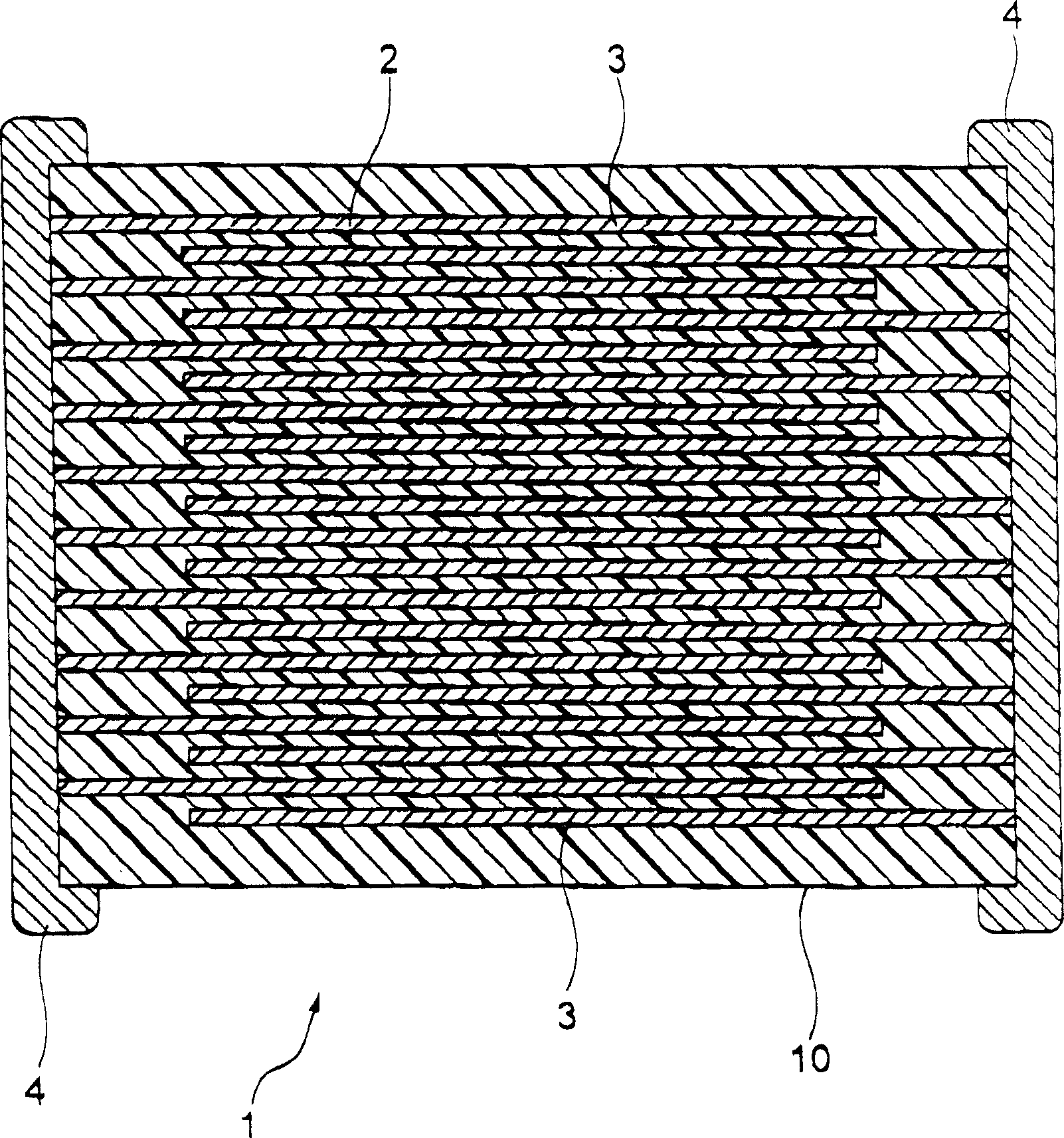
technical field [0001] The present invention relates to a dielectric ceramic composition used, for example, as a dielectric layer of a multilayer ceramic capacitor, and an electronic device using the dielectric ceramic composition as a dielectric layer. Background technique [0002] Produced as Multilayer ceramic capacitors are examples of electronic devices. The internal electrode layer of the multilayer ceramic capacitor is integrated with the ceramic dielectric by firing, so it is necessary to select a material that does not react with the ceramic dielectric. Therefore, platinum, palladium and other noble metals have conventionally been inevitably used as materials constituting the internal electrode layers. [0003] However, in recent years, dielectric ceramic compositions have been developed in which nickel and other inexpensive base metals can be used and extensive cost reductions have been achieved. [0004] In recent years, as the density of electronic circuits ha...

Claims


Application Information

Patent Timeline
Patent Type & Authority Patents(China)
IPC IPC(8): C04B35/468H01B3/12H01G4/12C01G23/00C01G31/00C01G45/00C04B35/622
CPCC04B2235/79C04B2235/3418C04B2235/5445C04B2235/652C01G45/006C04B2235/3436C04B35/64C04B2235/3225C04B2235/3217C04B2235/6562C04B2235/3262C01G31/006C04B2235/6567C04B2235/6588H01G4/1227C04B2235/72C01P2002/50C04B2235/663C04B2235/3208C04B35/4682C01P2006/40C04B2235/3454C04B2235/3241C01G23/003C04B35/638C04B35/62218C04B2235/3256C04B2235/3206C04B2235/3215C04B2235/3224C01G23/006C01P2004/03C04B2235/6584C01P2004/61C04B2235/3239C04B2235/6582C04B2235/3213C04B2235/6565C04B2235/664C04B2235/3258C01P2004/80H01G4/12
Inventor 堀江优作中野幸惠增宫薰里
Owner TDK CORPARATION
Learn More