Method for mfg multilayer printed circuit board and composite foil for use therein

A multi-layer printing and composite sheet technology, which is applied in the manufacture of printed circuit precursors, printed circuits, printed circuits, etc., can solve problems such as inability to extend copper layers, small diameters, and low laser energy, and achieve less processing equipment and high productivity , The effective effect of the manufacturing process

Inactive Publication Date: 2002-04-10
CIRCUIT FOIL LUXEMBOURG R L
View PDF1 Cites 13 Cited by
  • Summary
  • Abstract
  • Description
  • Claims
  • Application Information

AI Technical Summary

Problems solved by technology

However, if the copper layer at the point of incidence is 7 μm, then the set laser energy is too small, and the resultin

Method used


Image

  • Method for mfg multilayer printed circuit board and composite foil for use therein
  • Method for mfg multilayer printed circuit board and composite foil for use therein
  • Method for mfg multilayer printed circuit board and composite foil for use therein

Examples


Embodiment Construction

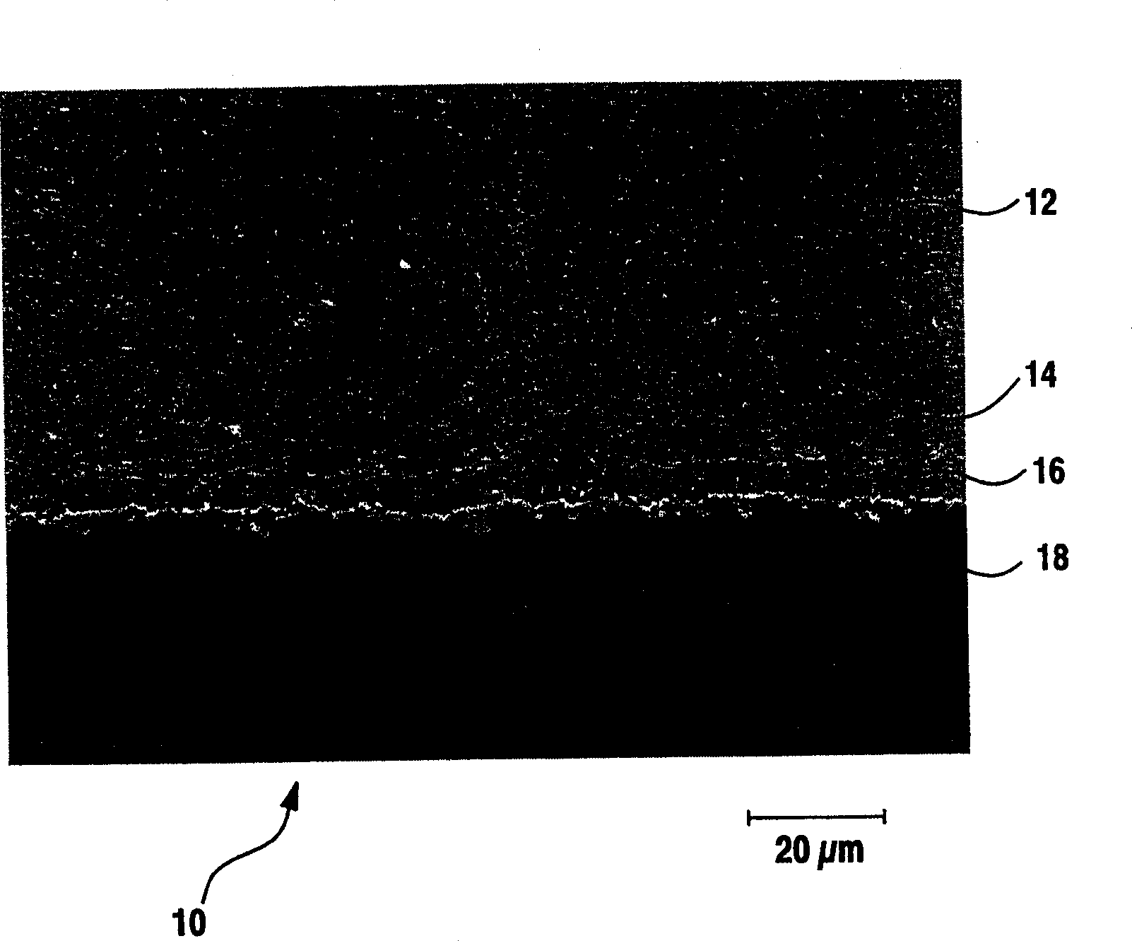
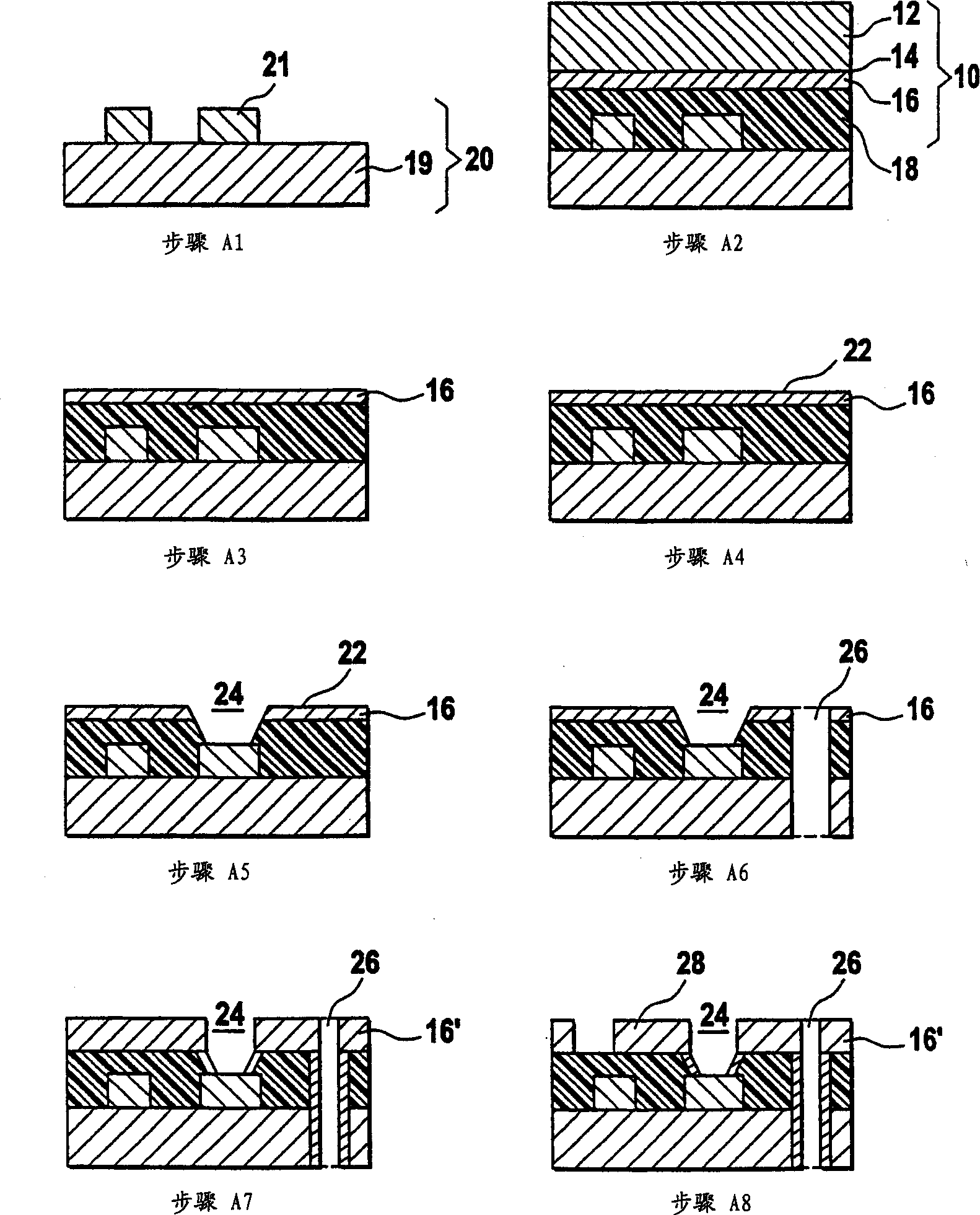
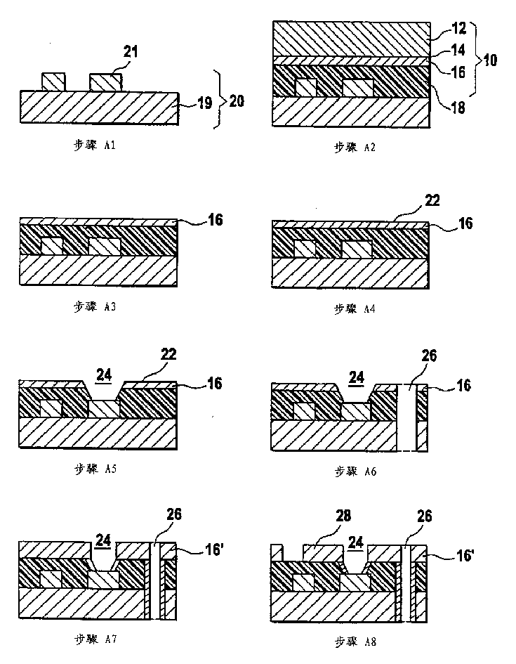
[0028] The present method uses a composite sheet 10, more specifically a resin-coated copper foil of a mounting carrier, to manufacture a multilayer PCB. figure 1 A scanning electron micrograph of such a composite sheet is shown, which will be laminated on a core plate. It consists of four distinct layers: carrier 12 ; release layer 14 ; working copper foil 16 ; and resin coating 18 . This composite sheet is the result of two consecutive manufacturing processes.

[0029] The first process is similar to that described in US3,998,601. First, a 70 μm thick slide 12 was fabricated by continuous electrodeposition from an acid-based electrolyte on a rotating titanium cylinder with a precisely designed surface. The surface topography of the barrel dictates and controls the initial copper layer deposited. The surface topography of the other side of the carrier layer - the rough side - is controlled by additives in the alkaline barrel electrolyte. In a further step, a release layer...


PUM

PropertyMeasurementUnit
Thicknessaaaaaaaaaa
Thicknessaaaaaaaaaa
Thicknessaaaaaaaaaa

Abstract

A method for manufacturing a multilayer printed circuit board is disclosed. First a composite foil (10) including a functional copper foil (16) mounted on a carrier foil (12) is laminated on a core board (20). The functional copper foil (16) is less than 10 mu m thick, and has a front side facing the carrier foil (12) and a back side coated with a resin (18). Next, the carrier foil (12) is removed from the functional copper foil (16), in order to uncover the front side of the functional copper foil (16). Then, a CO2 laser source is used to drill holes through the functional copper foil (16) and the resin (18) in order to form micro holes (24). It is also disclosed a composite foil (10) comprising four different layers for use in the manufacture of a multilayer printed circuit board.

Description

technical field [0001] This invention generally relates to the manufacture of multilayer printed circuit boards and composite sheets for use therein. Background technique [0002] The development of very compact and high-power electronic devices is due to the high-density printed circuit boards (PCBs) obtained with sequential build-up (SBU) technology. Basically, a stacked multilayer circuit is a composition of several overlapping layers of different wiring densities, separated by dielectric layers, and interconnected by micro-blind vias with a diameter typically less than 100 μm. [0003] Today, there are mainly three different techniques available for the fabrication of microvias: (1) photochemical etching of photodielectrics; (2) plasma etching processes; and (3) the still relatively new laser drilling process. [0004] Laser drilling appears to be the most promising technique for producing microscopic holes. Currently, excimer, Nd-YAG and CO 2 Laser sources are used t...

Claims


Application Information

Patent Timeline
IPC IPC(8): H05K3/00H05K3/02H05K3/38H05K3/46
CPCH05K3/0038H05K2203/0315Y10T29/49165H05K3/4652Y10T29/49155H05K2201/0323Y10T29/49126H05K3/385H05K3/025H05K2201/0112H05K3/46
Inventor 雷蒙德·盖尔斯达米恩·米歇尔
Owner CIRCUIT FOIL LUXEMBOURG R L
Why Eureka
Try Eureka