Multispectral imaging gene chip scanning instrument

A multi-spectral imaging and gene chip technology, applied in emission spectroscopy, instruments, spectrometry/spectrophotometry/monochromator, etc., can solve the problems of high cost, complexity, volume, and power consumption of the whole machine. Achieve the effect of saving inspection time, improving resolution and accuracy, and simplifying scanning direction

Inactive Publication Date: 2002-10-23
SHANGHAI INST OF OPTICS & FINE MECHANICS CHINESE ACAD OF SCI
View PDF0 Cites 15 Cited by
  • Summary
  • Abstract
  • Description
  • Claims
  • Application Information

AI Technical Summary

Problems solved by technology

Its size and power consumption are relatively large
[0006] In addition, the above-mentioned prior art [1] and [2] these two kinds of gene chip scanners with PMT and CCD as detection elements also have some common shortcomings: for example, the object to be detected or the excitation laser beam must have two directions of XY The detection task can only be completed by the translational movement of the chip scanner, so the chip scanner must have a multi-dimensional motion mechanism; the obtained images need to be spliced ​​after computer data processing, and the accuracy of the motion mechanism and the positioning accuracy of the motion mechanism are very high. The process also becomes more complicated; the scanning of the whole chip takes a long time, so the efficiency is low; the cost of the whole machine is relatively expensive, etc.

Method used


Image

  • Multispectral imaging gene chip scanning instrument
  • Multispectral imaging gene chip scanning instrument
  • Multispectral imaging gene chip scanning instrument

Examples


Embodiment Construction

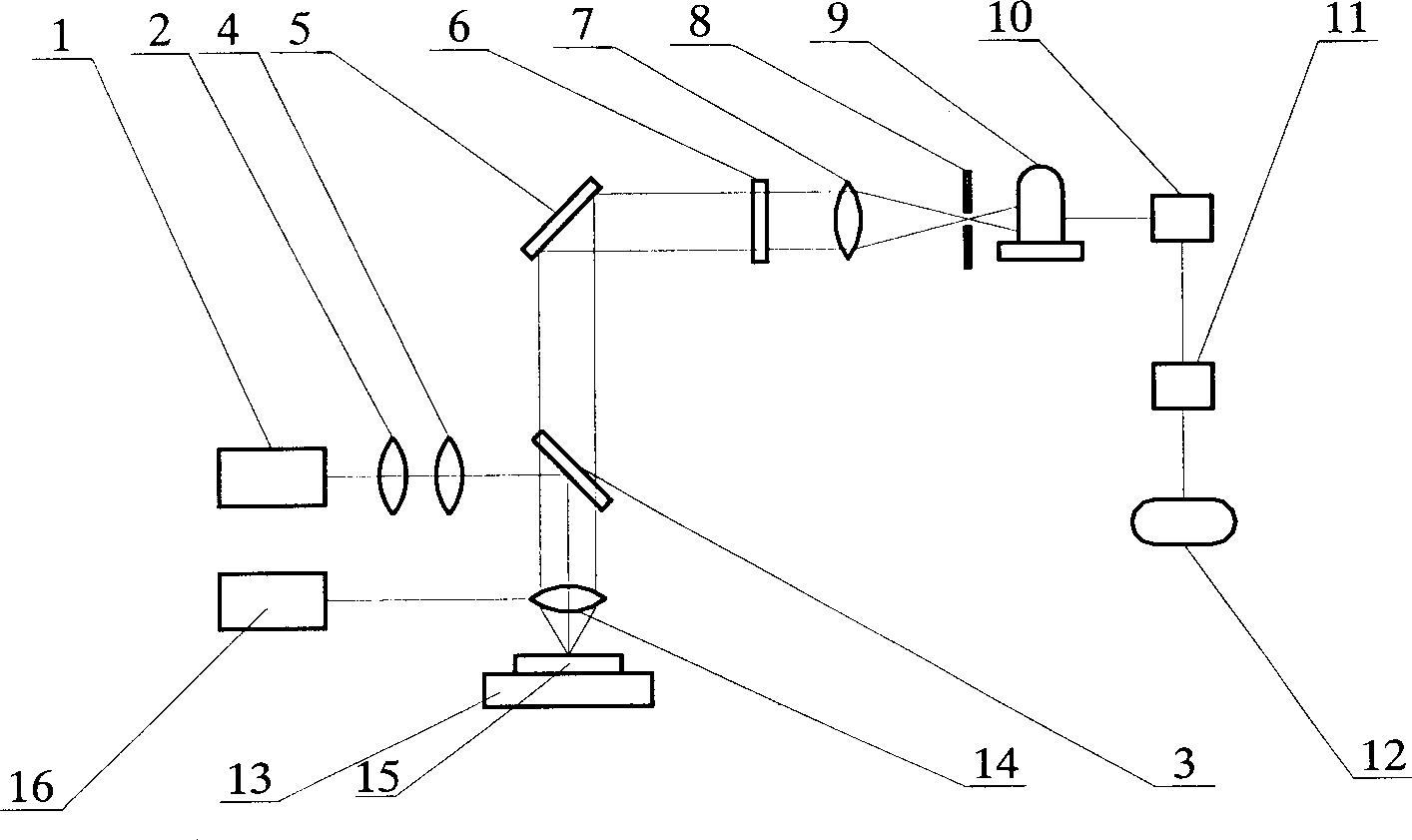
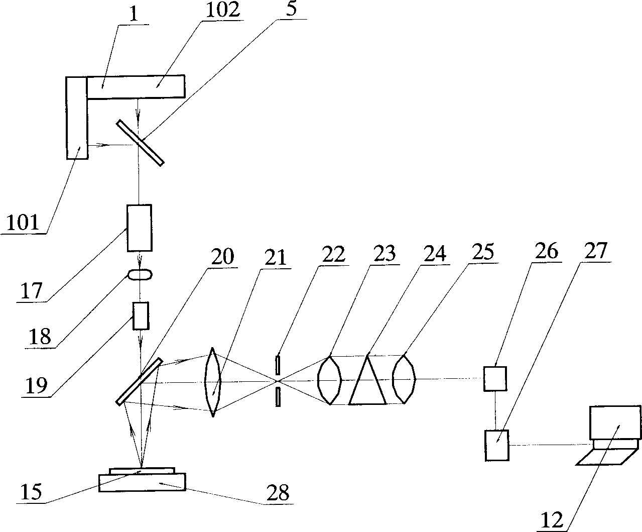
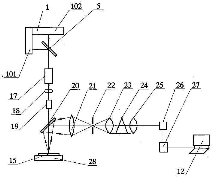
[0017] Such as figure 2 The structure of a biological gene chip scanner is shown. In the present invention, the photographing optical system 21 is a camera lens, f: 85mm, F2, Jupiter brand, and the effective field of view at the best image plane position is greater than the CCD receiving surface size of the line array. Wherein the laser light source 1 uses a dual-wavelength laser excitation: one is a semiconductor laser with a wavelength of 650nm for the laser light source 102, which can excite Cy5 fluorescent dyes; The 532nm wavelength output by frequency doubling of YAG) laser can excite Cy3 fluorescent dye. These two beams of laser light can be reflected and transmitted by the dichromatic reflector 5 (total reflection of 45 degrees incident on 532nm wavelength, and total transmission of 45 degrees incident on 650nm wavelength). , and then through a linear shaper 19 combined by a prism and an aspheric cylindrical lens to focus and form a linear illumination beam through a...


PUM


Abstract

The gene chip scanister mainly is used for detecting fluorescently-labeled post-hybridization gene biological chip, including the following steps: a laser beam is saped by linear shaper and passed through a reflector with slit to form a linear laser beam on the tested chip; the optical signal fed back by tested chip is passed through the reflector with slit and reflected, then passed through a photographic optical system and image in the slit diaphragm position; when it is excited by using laser beam with multiple wavelength, said signal is further passed through first imaging lens, dispersing element and second imaging lens and reflected on the detector of electric charge coupler with face array or line array. As compared with existent technology, it not only can simplify scanning direction, save detection time, but also can raise the resolution and accuracy of the detection.

Description

Technical field: [0001] The invention relates to a multispectral imaging gene chip scanner, in particular to a gene chip scanner using laser push-broom multispectral imaging. It is mainly used for detection after hybridization of fluorescently labeled gene biochips. It is generally believed that through the scanning and detection of biochips, including the comparison and analysis of the obtained signals by using corresponding software, people can take advantage of the advantages of high-throughput, simplicity, miniaturization, multi-parameters, intensification, and parallelization of gene chips. It opens up broad application prospects in many fields such as life science, basic medical research, disease diagnosis, new drug development, agriculture, food and environmental protection. Background technique: [0002] For fluorescently labeled biological gene chips, special gene scanners are required for post-hybridization detection. At present, dedicated gene chip scanners are ...

Claims


Application Information

Patent Timeline
Patent Type & Authority Applications(China)
IPC IPC(8): G01J3/06G01N21/64
Inventor 胡企铨王文奎刘敏
Owner SHANGHAI INST OF OPTICS & FINE MECHANICS CHINESE ACAD OF SCI
Why Eureka
Try Eureka