Glass passivating method for preparing RF mesa Si diode

A silicon diode and glass passivation technology, applied in semiconductor/solid-state device manufacturing, electrical components, circuits, etc., can solve the problems of difficult to form conformal film, low work efficiency, complexity, etc., and achieve good consistency, convenient operation, high efficiency effect

Inactive Publication Date: 2003-02-19
信息产业部电子第五十五研究所
View PDF0 Cites 7 Cited by
  • Summary
  • Abstract
  • Description
  • Claims
  • Application Information

AI Technical Summary

Problems solved by technology

The advantage of this method is that it has high precision and can be applied to shallow junctions (such as X j =0.5μm~5.0μm) devices, the disadvantages are high requirements for glass particle size and uniformity, sensitivity to the cleanliness of electrophoretic fluid (referring to ionic contamination), low work efficiency, poor repeatability, and difficulty in forming common Formed film, especially in the case of high table, the glass layer at the top corner of the thermoforming backstage is thin, it is difficult to play a good role in purifying the shallow junction
[0006] 2. Scratch coating method, which is to make a viscous liquid with a certain concentration of glass powder and adhesive, and evenly spread it on the surface of the silicon sample when using it, then scrape the glass on the top of the table with a scraper, and keep the side of the table and the table. Bottom glass, this method has the advantages of simple process operation, good repeatability, and high efficiency. The disadvantage is that the corners of the top of the table are not protected due to shrinkage after the glass powder is sintered and thermoformed. This method is only suitable for deep junction devices (such as deep junction devices) x j =15μm~25μm)
[0007] Before the present invention, the first SiO2 was used in the manufacture of radio frequency desktop high-voltage high-power silicon diodes abroad 2 Passivation protection, and then add the method of scratch coating glass passivation to solve the problem of P at the corner of the high table top + N - However, this method not only requires two different passivation processes, which is complicated, but also the corners of the mesa shrink after the glass powder is sintered and thermoformed, and in some places there is often only SiO 2 Purifying as the glass has shrunk below the shallow junction

Method used


Image

  • Glass passivating method for preparing RF mesa Si diode
  • Glass passivating method for preparing RF mesa Si diode
  • Glass passivating method for preparing RF mesa Si diode

Examples


Embodiment 1

[0024] Example 1: PIN Switching Diode

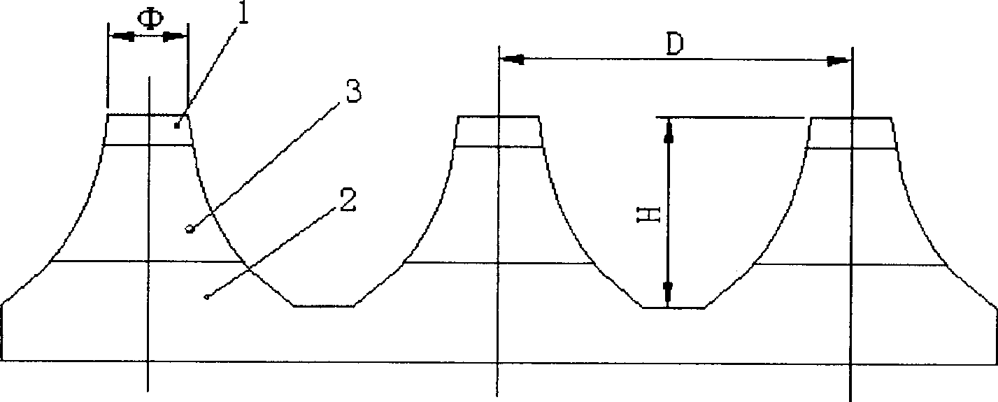
[0025] Chip size Mesa diameter Φ 135μm~150μm

[0026] Mesa height H 35μm~40μm

[0027] Adjacent die spacing D 330μm

[0028] P + N - Junction depth 1.0μm~2.0μm

[0029] N - Layer thickness 15μm~20μm

[0030] N + N - Junction depth 100μm~120μm

[0031] Process steps:

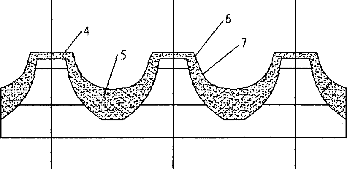
[0032] 1. Strict chemical cleaning and drying of the corroded wafers.

[0033] 2. Use a dropper to evenly coat the prepared glass slurry on the surface of the silicon wafer.

[0034] 3. Use a scraper to scrape off the glass slurry along the top of the table.

[0035] 4. Dry under infrared lamps to form a pre-deposited glass powder layer that undulates along the table.

[0036] 5. Send the silicon wafer into the high-temperature furnace, degas it in the degassing temperature zone of 550°C-580°C for 10 minutes, then enter the softening zone of the glass at 700°C-800°C, and preform for 10 minutes to form ...

Embodiment 2

[0039] Example 2: PIN Attenuation Diode

[0040] Chip size Mesa diameter Φ 85μm~95μm

[0041] Mesa height H 40μm~50μm

[0042] Adjacent die spacing D 330μm

[0043] P + N - Junction depth 2.8μm~3.2μm

[0044] N - Layer thickness 15μm~20μm

[0045] N + N - Junction depth 100μm~120μm

[0046] Process steps:

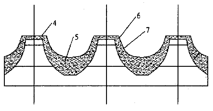
[0047] 1. Strict chemical cleaning and drying of the corroded wafers.

[0048] 2. Use a dropper to evenly coat the prepared glass slurry on the surface of the silicon wafer.

[0049] 3. Use a scraper to scrape off the glass slurry along the top of the table.

[0050] 4. Dry under infrared lamps to form a pre-deposited glass powder layer that undulates along the table.

[0051] 5. Send the silicon wafer into the high-temperature furnace, degas it in the degassing temperature zone of 550°C-580°C for 10 minutes, then enter the softening zone of the glass at 700°C-800°C, and preform for 15 minutes to form ...


PUM


Abstract

This invention provides a preparation method of RF desk silicon diode glass passivation with the following steps: a. coating uniformly the prepared glass slurry on the RF desk silicon diode surface b. removing the glass slurry with a scraping knife along the desk surface c drying to form a fluctuated predeposition glass powder layer along the desk surface d. sending samples into a high temperature oven to form preformed glass passive films under the temp of softening glass e repeating the above steps at least on time, finally sending the sample into the high temperature over dealt with heat forming treatment under glass forming temp.

Description

technical field [0001] The invention belongs to the technical field of surface passivation of silicon devices, and is mainly applied to the surface passivation of radio frequency desktop silicon diodes. Background technique [0002] Traditional RF silicon diodes mostly use SiO 2 or SiO 2 -Si 3 N 4 The double dielectric film is used as the surface passivation protection of the device to ensure that the device can work stably and reliably. The glass membrane used is on SiO 2 The basic structure of the membrane - interstitial fixed ions are added to the network structure of the silicon-oxygen tetrahedron, resulting in a denser microstructure and better resistance to external ionic contamination. The side can form a negatively charged center, which can effectively block the mobile ions on the silicon surface (such as Na + ) electromigration, and because it can be made into a thick film, it has strong performance against moisture and mechanical damage. Therefore, at present...

Claims


Application Information

Patent Timeline
IPC IPC(8): H01L21/31
Inventor 林立强刘萍
Owner 信息产业部电子第五十五研究所
Why Eureka
Try Eureka