

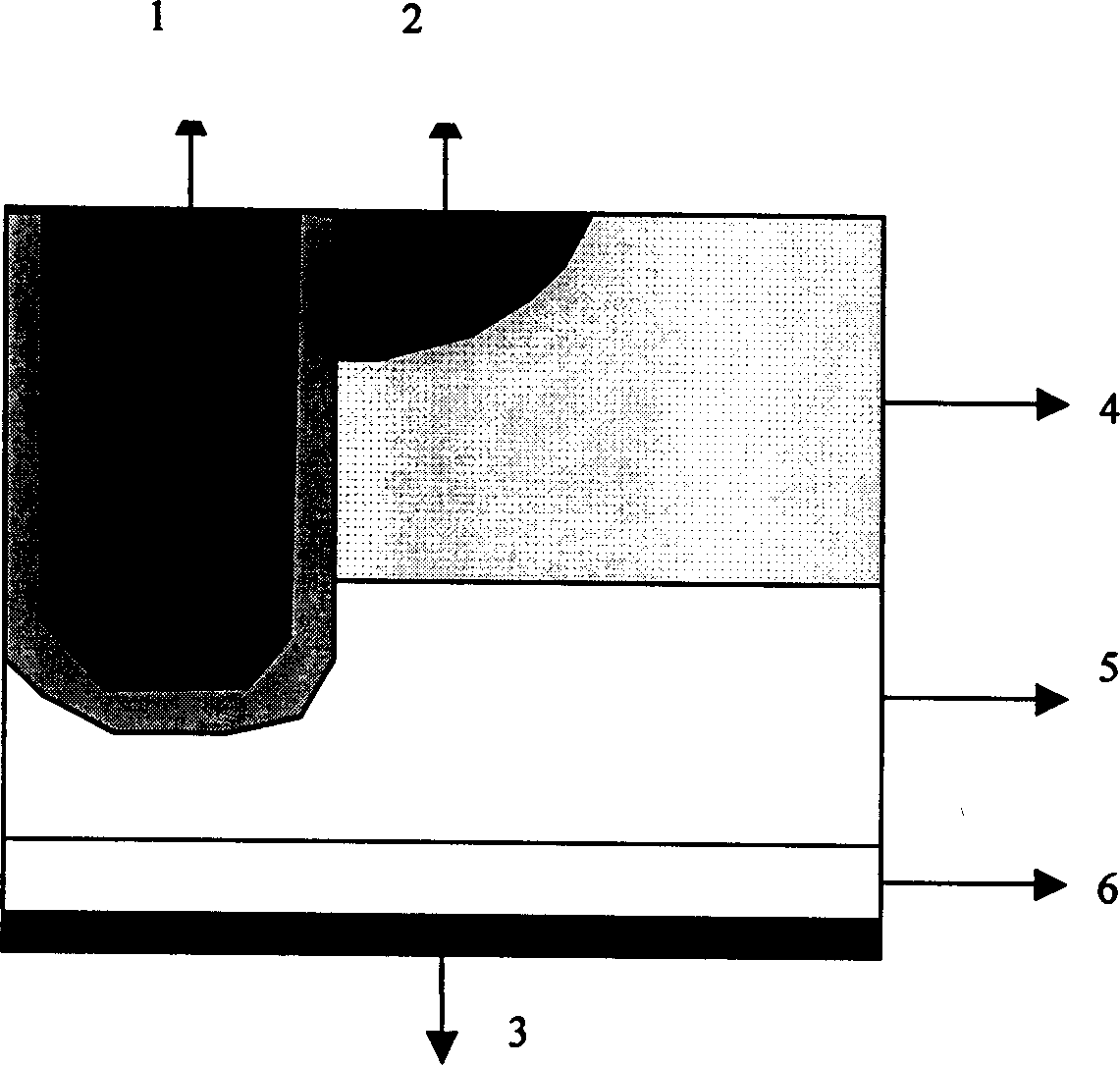
Vertical high-power field-effect transistor unit structure
A field-effect transistor and cell structure technology, applied in electrical components, semiconductor devices, semiconductor/solid-state device manufacturing, etc., can solve the problems of reducing device switching speed, large gate parasitic capacitance, and increasing circuit cost, and achieve a reduction in Effects of on-resistance, thermal impedance, small gate parasitic capacitance, and high withstand voltage
- Summary
- Abstract
- Description
- Claims
- Application Information
AI Technical Summary
Problems solved by technology
Method used
Image

Examples
Embodiment Construction
[0016] The present invention is further described below by way of examples.
[0017] 1. On an N-type (100) silicon substrate with a resistivity of 0.001 ohm-cm, epitaxy two layers of N-type thin layers by chemical vapor deposition, wherein the first epitaxial layer is adjacent to the silicon substrate and has a thickness of The thickness of the second epitaxial layer is 3.5 microns, and the resistivity is 0.3 ohm-cm. On the second epitaxial layer, a groove with a depth of 1.5-2.5 microns and a width of 1.0-1.5 microns is etched by plasma method.
[0018] 2. Thermally grow a layer of silicon dioxide on the silicon wafer with a thickness of 50 nanometers, and then deposit a layer of silicon nitride with a thickness of 150 nanometers by chemical vapor deposition. Then, a layer of photoresist masking film is formed by photolithography to expose the area where the trench is to be formed, and mask other areas with photoresist. The silicon nitride and silicon dioxide that are not m...
PUM
| Property | Measurement | Unit |
|---|---|---|
| Thickness | aaaaa | aaaaa |
| Thickness | aaaaa | aaaaa |
| Depth | aaaaa | aaaaa |
Abstract
Description
Claims
Application Information