Process flow of improved tungsten plug structure
A process flow, tungsten hexafluoride technology, applied in electrical components, semiconductor/solid-state device manufacturing, circuits, etc., can solve the problems of high cost and expensive tungsten hexafluoride, reduce costs and improve substrate adhesion , the effect of improving productivity
Inactive Publication Date: 2003-11-12
SHANGHAI INTEGRATED CIRCUIT RES & DEV CENT +1
View PDF0 Cites 5 Cited by
- Summary
- Abstract
- Description
- Claims
- Application Information
AI Technical Summary
Problems solved by technology
[0008] Tungsten hexafluoride is a very expensive gas with high cost
The standard DC magnetron sputtering cannot meet the above requirements, but some new technologies must be added, such as bias sputtering, long-range sputtering, metal plasma sputtering, radio frequency sputtering, etc.
Method used
View moreImage
Smart ImageViewing Examples
Examples
Embodiment Construction
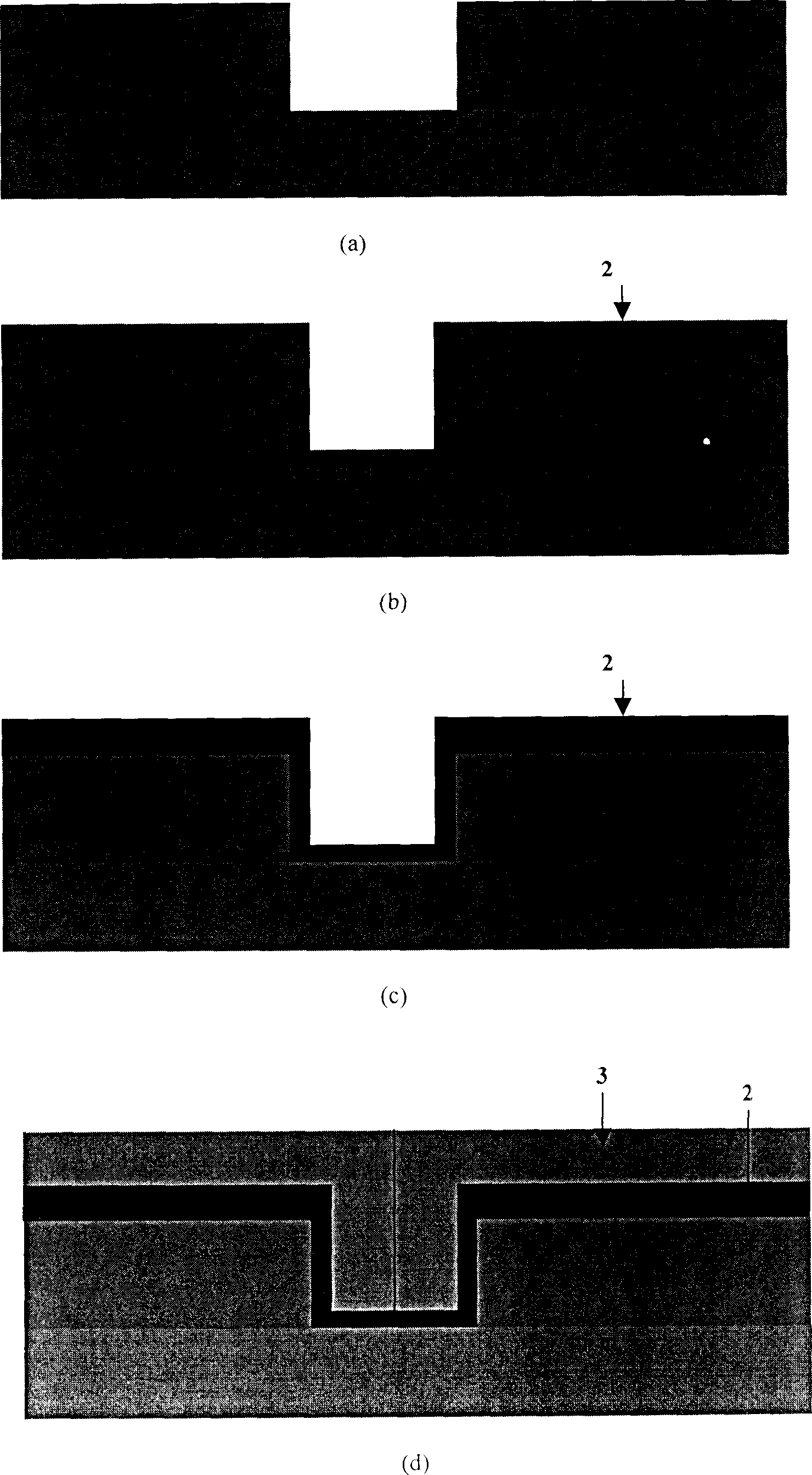
[0049] The main implementation steps of the present invention are as follows ( image 3 ):
[0050] 1. Use integrated circuit technology to form contact holes and butt holes (such as image 3 (a));
[0051] 2. Physical vapor deposition deposits tungsten, tungsten compounds and their combinations. Including: preheating; reverse sputter etching to remove the natural oxide layer and other residues in the contact hole and the butt hole; sputtering; (such as image 3 (b))
[0052] 3. Complete annealing in vacuum or in an atmosphere of argon, nitrogen and their combinations (such as image 3 (c));
[0053] 4. Use hydrogen as a reducing agent to reduce tungsten hexafluoride to fill contact holes and butt holes (such as image 3 (d)).
Login to View More PUM
| Property | Measurement | Unit |
|---|---|---|
| thickness | aaaaa | aaaaa |
Abstract
Traditional technique has the feaures of good fill effect and high integrity. But, the technique also has the disavantages of complex procedures, expensive cost and low production efficiency. The outstanding disavantage is that multiple steps are needed in the method for depositing titanium and titanium nitride as well as for depositing tungsten in chemical vapor deposition. The invented modified technological flow deposits tungsten and its compound as a diffusion barrier layer by using physical vapour phase process. Than, tungsten hexafluoride is hydrogen reducted to fill the opposite joint contact hole and opposite joint hole so as to simplify the flow, increase productivity and security, lowers cost.
Description
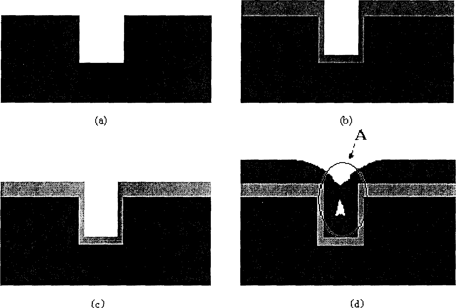
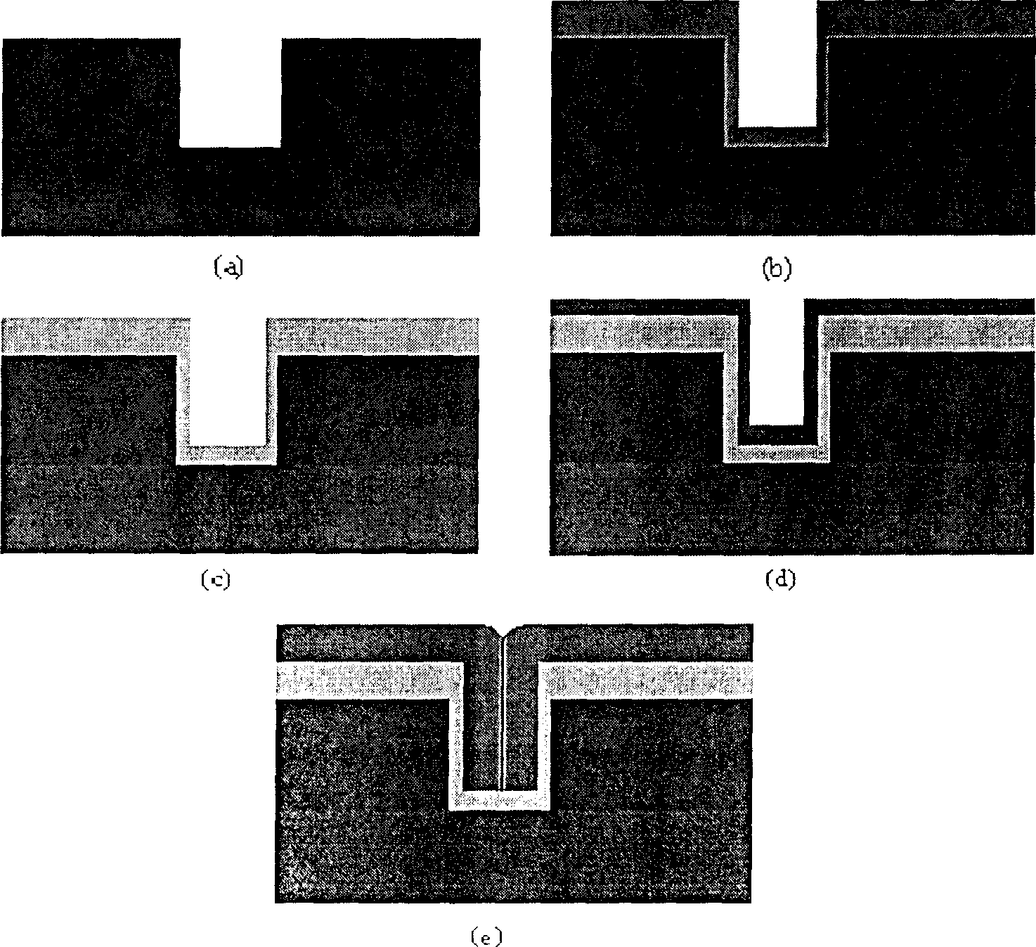
Technical field [0001] The invention belongs to the technical field of integrated circuit technology, and specifically relates to an improved manufacturing process flow of a tungsten pin structure. Background technique [0002] In the process of semiconductor integrated circuits, metallization is involved in the signal extraction of transistors. Reliable contacts, interconnections and metal lines at all levels are one of the keys to ensure the effective operation of transistors. The earliest realization is the aluminum metallization process, that is, first use the physical vapor deposition method to deposit titanium and titanium nitride double-layer film as the diffusion barrier layer, and then use the physical vapor deposition method to deposit the aluminum alloy. The simple process is as figure 1 Shown. The use of the diffusion barrier layer is to avoid inter-diffusion between aluminum and silicon in the future high-temperature alloy process, resulting in aluminum nails in the...
Claims
Login to View More Application Information
Patent Timeline
 Patent Type & Authority Applications(China)
IPC IPC(8): H01L21/28H01L21/3205H01L21/768
Inventor 金虎陈俭
Owner SHANGHAI INTEGRATED CIRCUIT RES & DEV CENT


