Laminated capacitor and its mfg. method
A manufacturing method and technology of capacitors, applied in the direction of capacitor manufacturing, laminated capacitors, capacitors, etc., can solve the problem of not being able to be used as a capacitor
- Summary
- Abstract
- Description
- Claims
- Application Information
AI Technical Summary
Problems solved by technology
Method used
Image

Examples
Embodiment 1
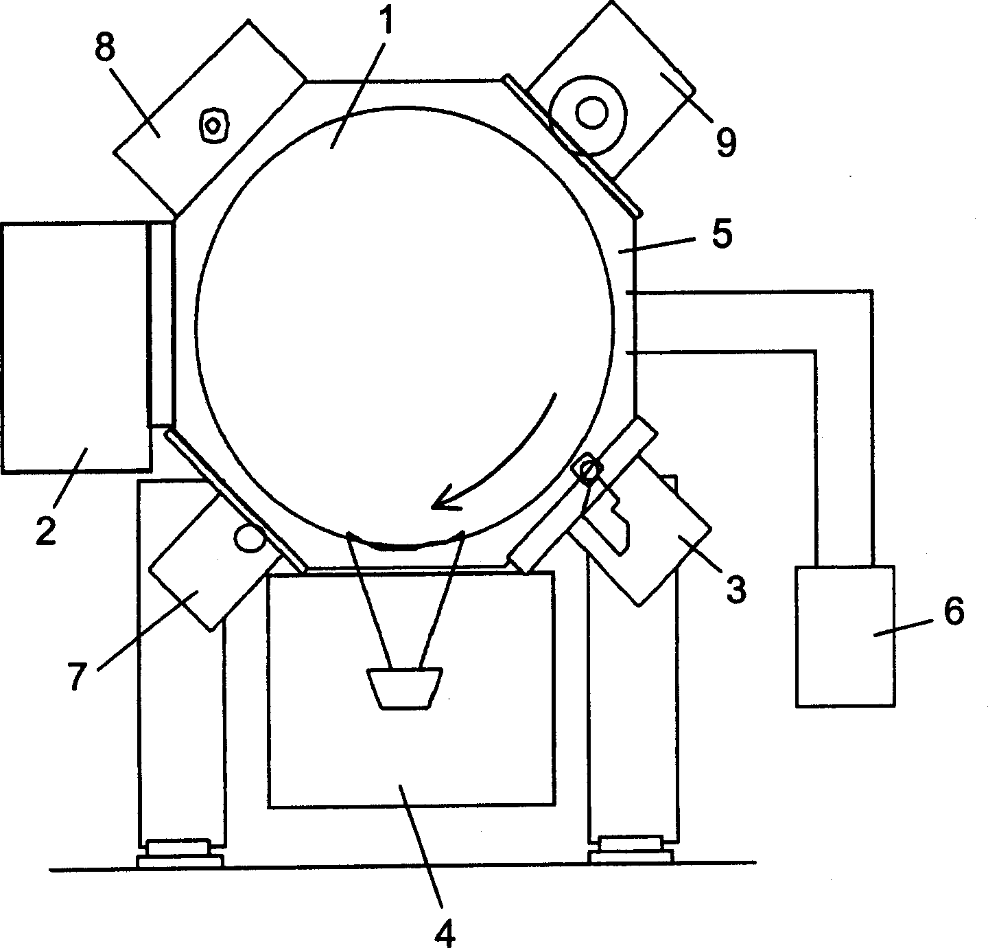
[0020] In Example 1, using figure 1 Devices were fabricated as indicated. figure 2 A~ figure 2 C represents the manufacturing process of the multilayer capacitor of the present invention. The degree of vacuum in the vacuum vessel 5 is set to 2×10 -2 Pa. The outer peripheral surface of the container drum 1 was kept at 5°C. As a reactive monomer for the dielectric material, dicyclopentadiene dimethanol diacrylate was used. The monomer is vaporized by the vapor deposition source 2 and deposited on the outer peripheral surface of the container drum 1 . In addition, any reactive monomer can be used as long as it is easy to vapor-deposit and the film after polymerization is good. Polyfunctional acrylates, polyfunctional methacrylates, polyfunctional vinyl ethers, and the like are preferably used.
[0021] Then, an electron beam curing device is used as the curing device 8 . And curing the deposited dielectric material. At this time, the thickness of the formed dielectric...
Embodiment 2
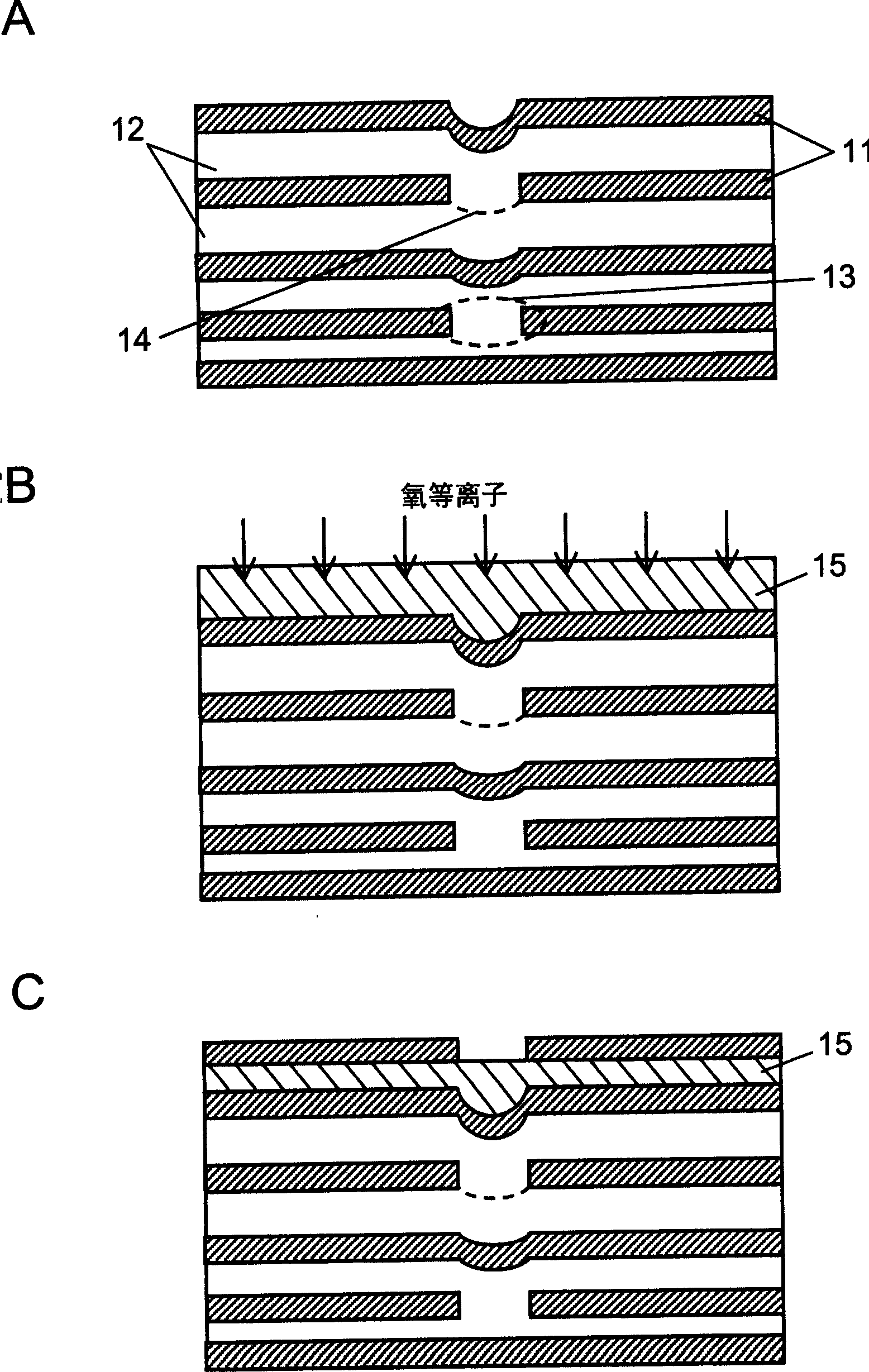
[0023] In Example 2, using figure 1 Devices were fabricated as indicated. All the same as in Example 1 up to step A. image 3 A indicates the state after process A is completed. Next, the procedure for flattening the electrical insulating portion recess 14 will be described. First, the metal vapor deposition source 4 is cut off with a shutter, and the resin layer 21 is formed by repeating lamination and curing 500 to 1000 times through the monomer vaporization source 2 and the curing device 8 . Then the monomer evaporation source 2 is cut off by the baffle. and, if image 3 As shown in B, the resin layer 21 is irradiated with argon plasma by the resin surface treatment device 9 . At this time, cutting is selectively performed from the corners of the recessed portion of the resin layer 21 , and finally the entire recessed portion can be buried with the resin layer 21 . and if image 3 As shown, the surface of the laminate can be flattened. In this embodiment, argon gas...
Embodiment 3
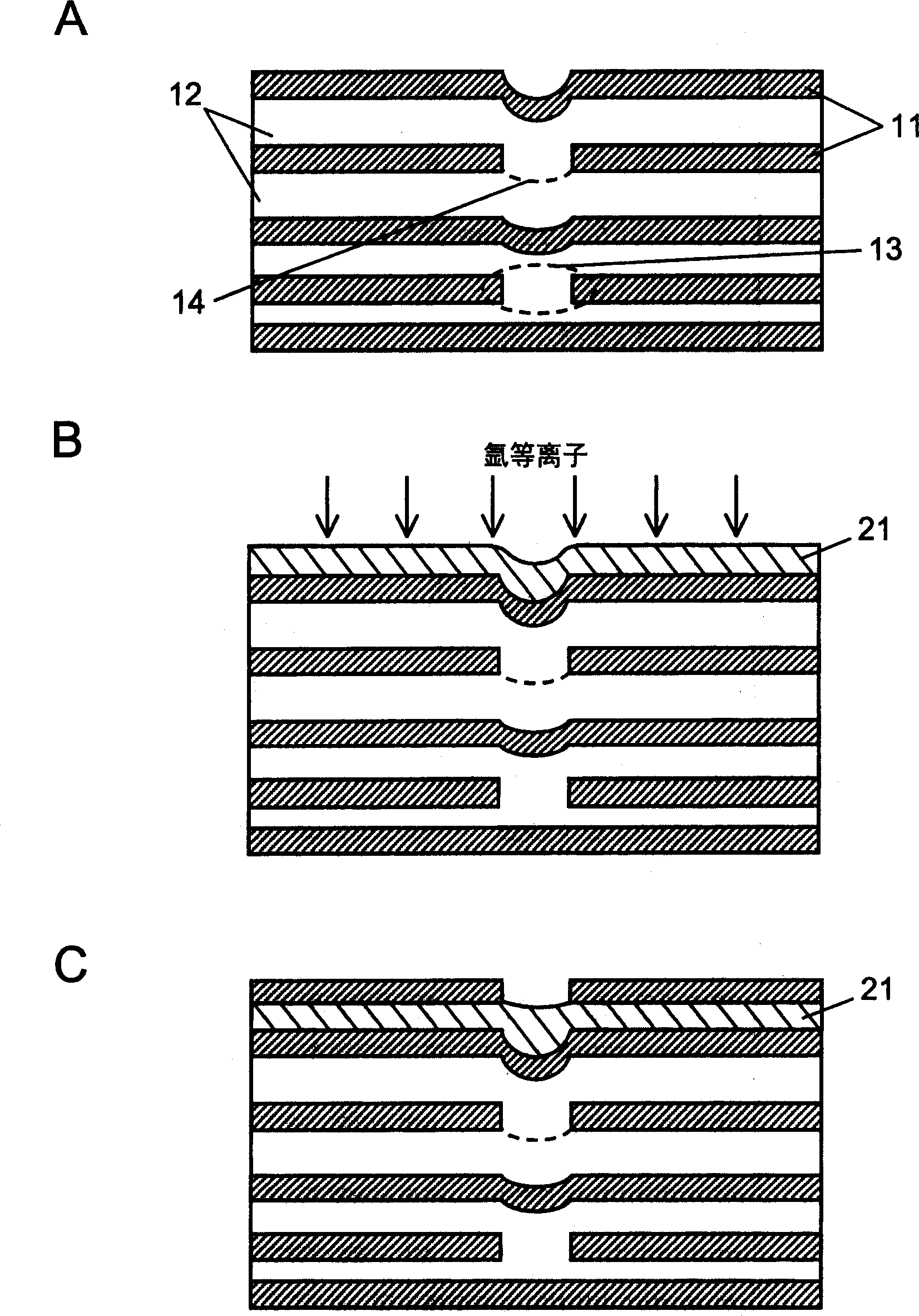
[0026] In Example 3, using figure 1 Fabrication setup shown. All the same as in Example 1 up to step A. Figure 4 A indicates the state after process A is completed. Next, the procedure for flattening the electrical insulating portion recess 14 will be described. First, the monomer vaporization source 2 is cut off by the shutter, and the metal vapor deposition source 4 is cut off by the pattern portion imparting shutter 31 . Then, if Figure 4 As shown in B, the metal layer 32 is laminated by passing through the patterned part and repeating about 500 to 1000 times. and if Figure 4 As shown in C, the concave portion produced by the electrical insulating portion is buried and the surface of the laminate is flattened. By repeating the above operations, a laminate of about 1.6 mm was formed. Starting from this laminate, a chip capacitor was obtained in the same manner as in Example 1. This chip capacitor has the same capacitor characteristics and solder heat resistance a...
PUM
| Property | Measurement | Unit |
|---|---|---|
| capacitance | aaaaa | aaaaa |
| electric potential / voltage | aaaaa | aaaaa |
Abstract
Description
Claims
Application Information
 - R&D
- Intellectual Property
- Life Sciences
- Materials
- Tech Scout
- Unparalleled Data Quality
- Higher Quality Content
- 60% Fewer Hallucinations
Browse by: Latest US Patents, China's latest patents, Technical Efficacy Thesaurus, Application Domain, Technology Topic, Popular Technical Reports.
© 2025 PatSnap. All rights reserved.Legal|Privacy policy|Modern Slavery Act Transparency Statement|Sitemap|About US| Contact US: help@patsnap.com