Unlock instant, AI-driven research and patent intelligence for your innovation.

Semiconducting process for ceramic chip of semiconductor ceramic capacitor

A technology of ceramic capacitors and process methods, which is applied in the direction of capacitors, capacitor manufacturing, and fixed capacitor dielectrics, etc., which can solve the problems of high cost, high risk, and poor process adaptability, etc., to reduce production costs, improve economic benefits, and reduce risks. Effect

Inactive Publication Date: 2004-03-31
广东南方宏明电子科技股份有限公司
View PDF2 Cites 0 Cited by
  • Summary
  • Abstract
  • Description
  • Claims
  • Application Information

AI Technical Summary

Problems solved by technology

The first method can guarantee the quality of the product, but the cost is undoubtedly high, and a reliable continuous supply must be agreed with the supplier, and the danger of transportation and storage of pure hydrogen must be resolved; the second method directly uses ammonia decomposition gas, Compared with the previous one, the cost is lower, but the hydrogen content of the decomposition gas is as high as 75%, and it is more dangerous to use it directly as a reducing gas in a high-temperature kiln, and because the best reducing sintering atmosphere of the grain boundary layer formula tile is in the range of 2 to 20%. Therefore, the ammonia decomposition gas cannot be used directly, and the process adaptability is poor

Method used


Image

  • Semiconducting process for ceramic chip of semiconductor ceramic capacitor
  • Semiconducting process for ceramic chip of semiconductor ceramic capacitor
  • Semiconducting process for ceramic chip of semiconductor ceramic capacitor

Examples


Embodiment Construction

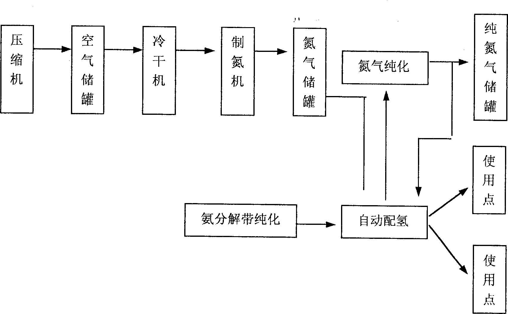
[0009] The semiconductor ceramic capacitor tile semiconducting process method is characterized in that: nitrogen and hydrogen mixed gas decomposed from pure nitrogen and liquid ammonia are used as the reducing and sintering atmosphere of the grain boundary layer semiconductor tile and the semiconducting of the surface layer semiconductor tile Restore the atmosphere. The pure nitrogen is produced by a nitrogen generator.

[0010] The reduction and sintering atmosphere of the grain boundary layer semiconductor tiles contains hydrogen in a proportion of 2% to 20%.

[0011] The semiconducting reduction atmosphere of the surface layer semiconductor tiles contains hydrogen in a proportion of 5% to 30%.

[0012] The present invention is realized by a set of gas supply system, and this gas supply system is divided into following five parts:

[0013] 1. Air compression and purification system:

[0014] The air compression and purification system consists of air compressors, filters ...


PUM


Abstract

The invention is a semiconductor processing method of superficial-layer and crystal boundary-layer semiconductor ceramic capacitor pieces. It adopts nitrogen and hydrogen mixed gas as sintering reducing atmosphere of the crystal boundary-layer capacitor and reducing atmosphere of the superficial-layer one. The proportion of hydrogen gas in the former atmosphere is 2-20%, and that in the latter atmosphere 5-30%. The producing technique is safe and reliable.

Description

Technical field: [0001] The invention relates to the technical field of ceramic capacitors, in particular to a process method for semiconducting ceramic chips of surface layer semiconductor ceramic capacitors and grain boundary layer semiconductor ceramic capacitors. Background technique: [0002] Semiconductor ceramic capacitors include surface layer and grain boundary layer. According to the IEC standard, they are type III ceramic capacitors. They have the advantages of small size and large capacity, and are widely used in electronic information products. The invention is aimed at the semiconducting processing method of the surface layer and the grain boundary layer of the semiconductor ceramic capacitor tile, and is one of the key processes for the production of the semiconductor ceramic capacitor. [0003] At present, manufacturers of type III ceramic capacitors in the world are represented by Japanese Murata Corporation (MURATA) and Japanese TDK Corporation (see US Pate...

Claims


Application Information

Patent Timeline
IPC IPC(8): H01G4/12
Inventor 章士瀛王振平王守士章仲涛
Owner 广东南方宏明电子科技股份有限公司
Features
  • R&D
  • Intellectual Property
  • Life Sciences
  • Materials
  • Tech Scout
  • Unparalleled Data Quality
  • Higher Quality Content
  • 60% Fewer Hallucinations
Learn More