Organic electroluminescence device with improved light-emitting efficiency

An electroluminescent device and organic technology, applied in electroluminescent light sources, electrical components, luminescent materials, etc., can solve the problems of limiting device expansion and limitation, and achieve improved efficiency, high luminous efficiency, and good carrier transport capability. Effect

Inactive Publication Date: 2004-04-28
BEIJING VISIONOX TECH
View PDF4 Cites 13 Cited by
  • Summary
  • Abstract
  • Description
  • Claims
  • Application Information

AI Technical Summary

Problems solved by technology

Although the above two technical solutions overcome some shortcomings in the traditional single doping system, improve the working life and luminous efficiency of the device to a certain extent, and may also improve the luminous efficiency and chromaticity stability of the device, but the actual In the application, the host and dopant materials that meet the requirements of its technical scheme are still limited
The dye used as doping needs to meet certain conditions from the perspective of energy band. Such materials need to be screened in the experiment. There are not many that meet the requirements of the device, and even fewer have high performance (good film-forming properties, high luminous efficiency, etc.). , thus often limiting the expansion of the device's color coordinates

Method used


Image

  • Organic electroluminescence device with improved light-emitting efficiency
  • Organic electroluminescence device with improved light-emitting efficiency
  • Organic electroluminescence device with improved light-emitting efficiency

Examples


Embodiment 1

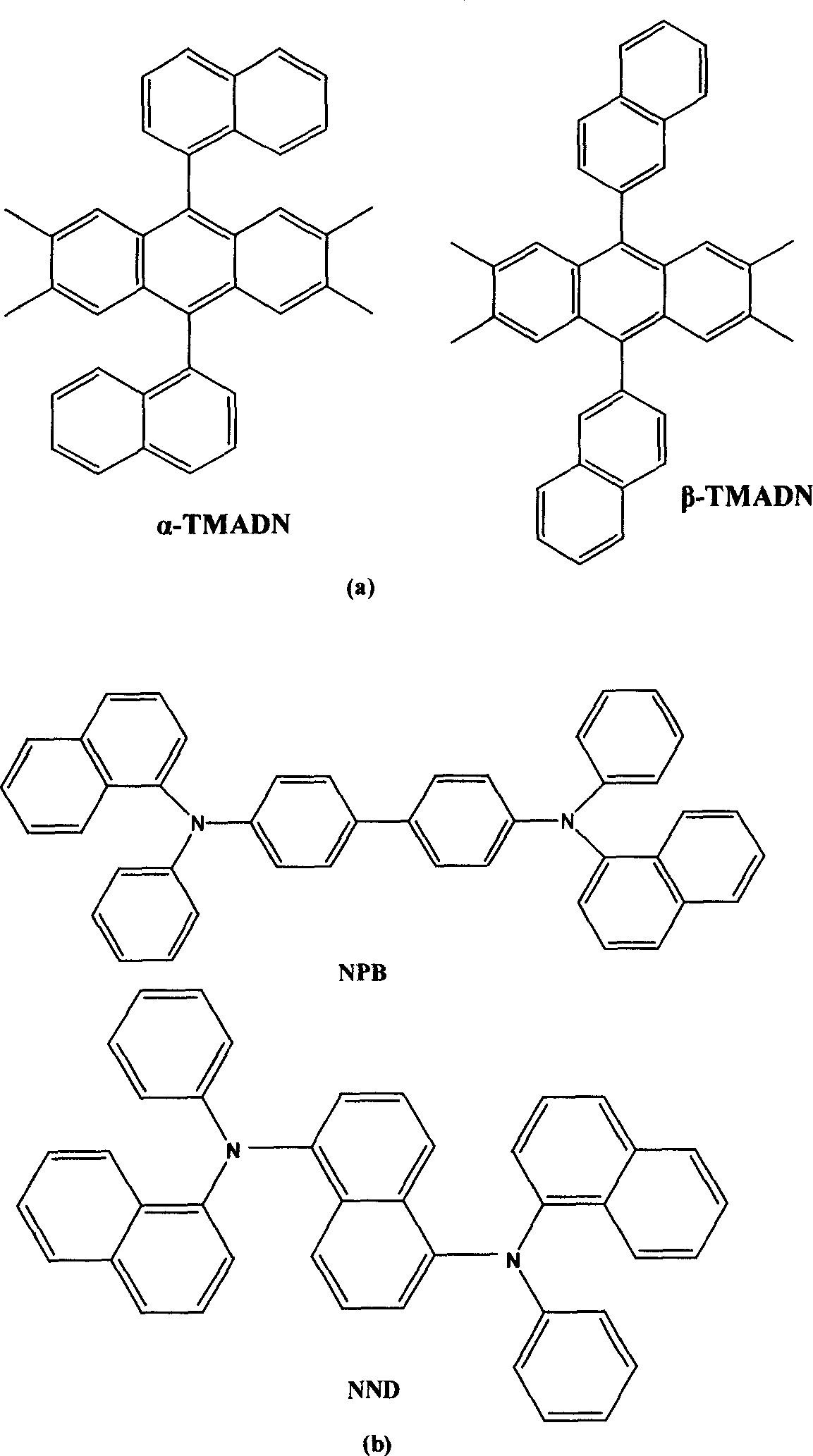
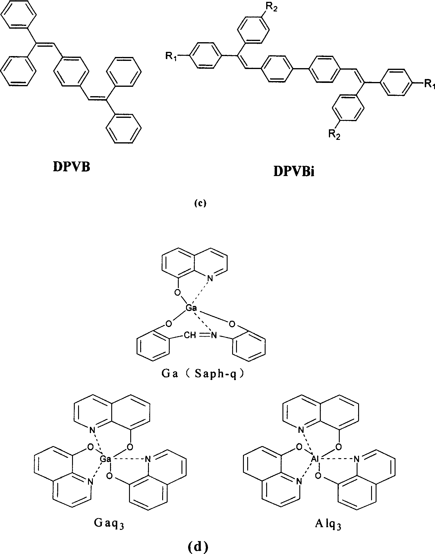
[0030] Preparation of device 1: Deposit a layer of indium oxide-tin oxide (ITO) as a transparent anode on a glass substrate, and then prepare a layer of 50 nm thick hole transport material by vacuum evaporation: N, N'- Diphenyl-N,N′-bis(1-naphthyl)-1,1′-biphenyl-4,4′-diamine (NPB) was then continued on this hole-transporting layer by vacuum evaporation of dual-source A layer of 15 nanometer thick material in the present invention, 2,3,6,7-tetramethyl-9,10-bis(1-naphthyl)anthracene (compound α-TMADN) and 2,3, 6,7-tetramethyl-9,10-bis(2-naphthyl)anthracene (compound β-TMADN), the concentration ratio is 9:1 (α-TMADN: β-TMADN), as the light-emitting layer; again here On the light-emitting layer, a layer of 40 nm-thick hole-transporting material and hole-blocking material 4,7-diphenyl-1,10-phenanthroline (BPhen) is continuously deposited by vacuum evaporation, and finally vacuum-evaporated A layer of Mg:Ag (1:10) alloy is used as the cathode of the device, about 200 nm. Add the p...

Embodiment 2

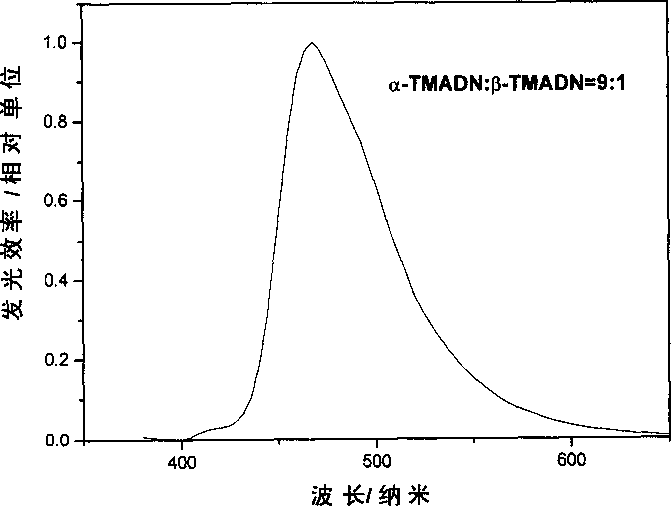
[0032]A group of devices were prepared according to the preparation method and steps of Example 1, and the light-emitting layer materials were also 2,3,6,7-tetramethyl-9,10-di(1-naphthyl)anthracene (compound α-TMADN) and 2,3,6,7-Tetramethyl-9,10-bis(2-naphthyl)anthracene (compound β-TMADN), adjust the concentration ratio of α-TMADN and β-TMADN, the device can achieve different luminous efficiencies , see attached Figure 5 .

Embodiment 3

[0034] Preparation of device 2: Deposit a layer of indium oxide-tin oxide (ITO) as a transparent anode on a glass substrate, and then prepare a layer of 50 nm thick hole transport material by vacuum evaporation: N, N'- Diphenyl-N,N′-bis(1-naphthyl)-1,1′-biphenyl-4,4′-diamine (NPB) was then continued on this hole-transporting layer by vacuum evaporation of dual-source A layer of material N, N'-diphenyl-N, N'-bis(1-naphthyl)-1,1'-biphenyl-4,4'-di Amine (NPB) and 1,5-bis[N-(naphthyl)-N-phenyl]naphthalene diamine (NND) in a concentration ratio of 7:1 (NPB:NND) as the light-emitting layer; On the layer, a layer of 40 nm-thick hole transport material and hole blocking material 4,7-diphenyl-1,10-phenanthroline (BPhen) was deposited by vacuum evaporation, and finally a layer of vacuum evaporation was deposited. A layer of Mg:Ag (1:10) alloy acts as the cathode of the device, about 200 nm. Add the positive electrode of direct current to the ITO layer, and add the negative electrode t...


PUM


Abstract

This invention relates to an organic electro-luminance device OLED containing a substrate, an anode and a cathode on it, and organic function layer between the anode and cathode including a luminance layer which is composed of two host materials to be isomer to each other or homogloue or analogue. This invention also provides a blue OLED device with the best luminance efficiency and colority. The host material of each component in this invented device luminance layer can be prepared by dual mixed steam, combination of the host materials can be luminance material directly or doped with dye as the carrier transfer materials.

Description

Technical field: [0001] This invention relates to organic electroluminescent devices, and in particular to the design of organic light-emitting layers for improved luminous efficiency. Background technique: [0002] With the development of multimedia technology and the advent of the information society, the performance requirements of flat panel displays are getting higher and higher. Three new display technologies emerging in recent years: plasma display, field emission display and organic electroluminescent display (OLED), all make up for the shortcomings of cathode ray tube and liquid crystal display to a certain extent. Among them, OLED has a series of advantages such as self-illumination, low-voltage DC drive, full curing, wide viewing angle, and rich colors. Compared with liquid crystal displays, OLED does not require a backlight, has a large viewing angle, low power consumption, and its response speed is faster than that of liquid crystal displays. It is 1000 times t...

Claims


Application Information

Patent Timeline
Patent Type & Authority Applications(China)
IPC IPC(8): C09K11/06H05B33/14H05B33/20
Inventor 邱勇王立铎阚莹段炼雷钢铁
Owner BEIJING VISIONOX TECH
Why Eureka
Try Eureka