Polymer-based waveguide device and method for fabricating the same

A manufacturing method and polymer technology, applied in the direction of optical waveguide light guide, laser components, optics, etc., can solve the problems of unsuitable waveguide amplifiers, long manufacturing cycle, increased optical loss, etc., to achieve increased concentration of rare earth metal ions and low cost , high gain effect

Inactive Publication Date: 2004-06-02
HONG FU JIN PRECISION IND (SHENZHEN) CO LTD +1
View PDF1 Cites 3 Cited by
  • Summary
  • Abstract
  • Description
  • Claims
  • Application Information

AI Technical Summary

Problems solved by technology

But this erbium-doped slab waveguide device 2 is not suitable for use as a waveguide amplifier because of its polarization dependence, and it not only generates optical amplification in the required linear direction, but also generates optical amplification in other directions of the plane, thereby increasing optical loss.
In addition, the manufacturing cycle of the waveguide device is longer, resulting in increased cost

Method used


Image

  • Polymer-based waveguide device and method for fabricating the same
  • Polymer-based waveguide device and method for fabricating the same
  • Polymer-based waveguide device and method for fabricating the same

Examples


Embodiment Construction

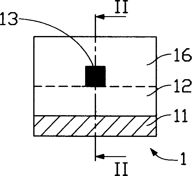
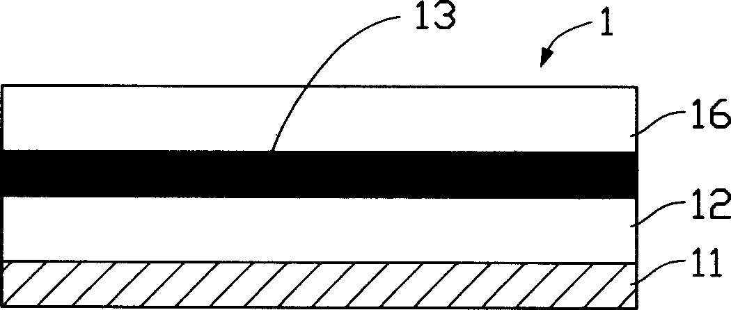
[0011] Please refer to figure 1 , the polymer-based waveguide device 1 of the present invention can be used as an optical amplifier or a laser waveguide, which includes a substrate 11 , a polymer inner cladding layer 12 , a polymer outer cladding layer 16 and a channel waveguide 13 . The polymer inner cladding layer 12 covers the substrate 11 , and the channel waveguide 13 is disposed on the polymer inner cladding layer 12 and wrapped in the polymer outer cladding layer 16 . Please also refer to figure 2 , the channel waveguide 13 is substantially parallel to the substrate 11 .

[0012] The manufacture of the polymer-based waveguide device 1 can be carried out in the following four steps:

[0013] (1) Prepare the substrate 11. The material of the substrate 11 can be single crystal silicon, polycrystalline silicon, lithium niobate single crystal, quartz, optical glass or optical resin, and be formed by the existing stretching or casting process;

[0014] (2) coating on the...


PUM


Abstract

The polymer-based waveguide device for light amplifier and laser waveguide includes base body, inner polymer coating on the base body, channel waveguide set on the inner polymer coating and outer polymer coating covering the inner polymer coating and the channel waveguide. The channel waveguide is made with at least one kind of RE metal ion doped composition capable of being excited to generate laser. The preparation process of the waveguide device includes the steps of: making a base body; painting the inner polymer coating on the base body and drying to cure; painting the second polymer with dissolved RE metal ion doped composition and selectively curing and etching to form the channel waveguide; and painting outer polymer coating and drying to cure. The waveguide device has excellent light amplifying and transmitting function.

Description

【Technical field】 [0001] The present invention relates to a waveguide device used as an optical amplifier or a laser waveguide and its manufacturing method, especially a polymer-based waveguide device used as an optical amplifier or a laser waveguide and its manufacturing method. 【Background technique】 [0002] In the process of making optical fiber, rare earth ions are doped into the optical fiber core as a gain medium, and the optical signal can be directly amplified by using pump light to provide optical gain. In the manufacture of optical fibers, the optical fibers made by doping erbium ions into the core are erbium-doped optical fibers, which are commonly used in Erbium-Doped Fiber Amplifier (EDFA), and can be directly connected to the The signal light is amplified and is the main component to provide optical gain. [0003] U.S. Patent No. 5,982,973 discloses an erbium-doped slab waveguide device 2, please refer to image 3 , which consists of a substrate 21, an inner ...

Claims


Application Information

Patent Timeline
Patent Type & Authority Applications(China)
IPC IPC(8): G02B6/12G02F1/39H01S3/00
Inventor 陈杰良吕昌岳
Owner HONG FU JIN PRECISION IND (SHENZHEN) CO LTD
Why Eureka
Try Eureka