Process for preparing nitridation carbon / carbon nanotubes and nano diodes and use thereof

A nano-diode and carbon nano-tube technology, which is applied in the manufacture of semiconductor/solid-state devices, electrical components, circuits, etc., can solve problems such as complex preparation methods, and achieve the effects of simple process, stable performance, and excellent rectification performance

Inactive Publication Date: 2004-08-18
INST OF CHEM CHINESE ACAD OF SCI
View PDF1 Cites 3 Cited by
  • Summary
  • Abstract
  • Description
  • Claims
  • Application Information

AI Technical Summary

Problems solved by technology

However, these preparatio

Method used


Image

  • Process for preparing nitridation carbon / carbon nanotubes and nano diodes and use thereof
  • Process for preparing nitridation carbon / carbon nanotubes and nano diodes and use thereof
  • Process for preparing nitridation carbon / carbon nanotubes and nano diodes and use thereof

Examples


Embodiment 1

[0040] The present invention prepares the method for carbon nitride / carbon nanotube nano diode:

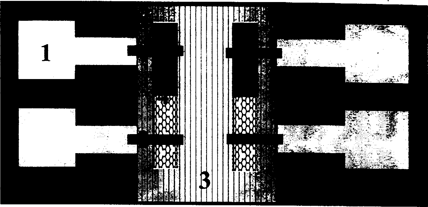
[0041] In the first step, thermally oxidized silicon dioxide (SiO 2 , 500 nanometers) 3 surface with a photolithographic technique to prepare a pair of Ti / Au electrode arrays, the electrode width is 1 micron, and the distance between the electrodes is 5-10 microns.

[0042] In the second step, the prepared carbon nitride / carbon nanotubes are then dispersed in carbon tetrachloride and dichlorobenzene solution, (the preparation method of carbon nitride / carbon nanotubes is referring to: Liu Yunqi, Hu Ping'an, Xiao Kai, Wang Xianbao , Fu Lei, Zhu Daoben, application number: 02160815.6), drop a suspension containing carbon tubes on silicon dioxide (SiO 2 )3 on the base.

[0043]The 3rd step, after the solvent volatilizes completely, put into the vacuum chamber of IDS P2X focused ion beam (FIB) system, observe the carbon tube on the substrate 3 (diameter is 50 nanometers, length 4 mi...

Embodiment 2

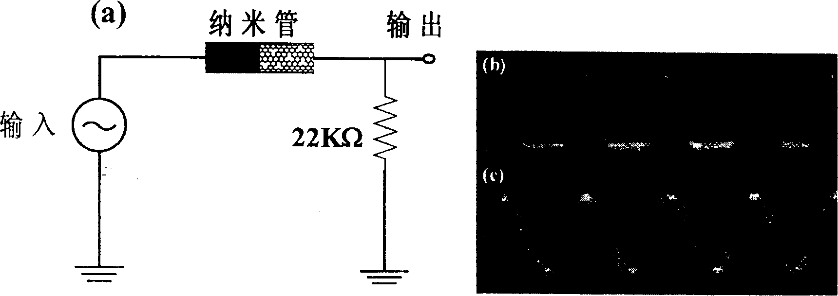
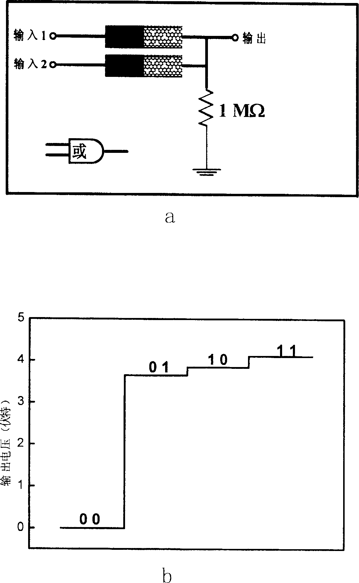
[0046] The present invention consists of a carbon nitride / carbon nanotube nanodiode to form a preparation method of a logic gate circuit:

[0047] In the first step, prepare two carbon nitride / carbon nanotube diodes according to the preparation method of Example 1;

[0048] In the second step, the prepared two carbon nitride / carbon nanotube diodes were connected with a resistance of 1 megohm according to image 3 a and Figure 4 The circuit diagram shown in a, respectively connected into a diode logic "or" (see image 3 a) and "and" (see Figure 4 a) Gate circuit, the resistance value of grounding and positive 5V resistance can be selected between 500K and 1.5 megohm, and the preferred value is 1 megohm.

[0049] Its logic output curve is as image 3 b and Figure 4 As shown in b. When one of the two input terminals is high level, the output is high level, which is an "or" gate circuit; and when both input terminals are high level, the output is high level, which is "and...

Embodiment 3

[0051] Application of the present invention in transistor radio:

[0052] Replace the silicon diode in the Sanyo RP1270 transistor radio with the carbonized nitrogen / carbon nanotube diode prepared according to embodiment 1 (see Figure 5 ), the radio can still clearly listen to different radio programs.


PUM

PropertyMeasurementUnit
Diameteraaaaaaaaaa
Lengthaaaaaaaaaa

Abstract

The invention relates to the method of making and use of nitrogenized carbon / carbon nano tubes having nano-junctions, and the process for preparing rectification circuit and logic gate circuit formed therefrom, the method in accordance with the invention comprises the steps of, (1) preparing nitrogenized carbon / carbon tube diode using IDS P2X focused ion beam system, (2) linking the obtained nitrogenized carbon / carbon nano tube diode, the signal oscillator, the dual-channel oscillography equipment and the resisters into a half-wave rectifying circuit, (3) linking the obtained nitrogenized carbon / carbon nano tube diode and the resister into logic OR-gate and AND-gate circuit, (4) replacing the wave detection diode of the transistor radio with the obtained nitrogenized carbon / carbon nano tube diode. The obtained nitrogenized carbon / carbon nano tube diode prepared by the method of the invention has stabilized performance, good rectification property and logical function.

Description

technical field [0001] The invention relates to a method for preparing a carbon nitride / carbon nanotube diode with a nano junction, and a method for preparing a rectifier circuit and a logic gate circuit. Background technique [0002] With the development of electronic technology, the size of electronic devices is constantly shrinking. However, when the size of the device enters the nanometer scale from the micrometer, due to the influence of the quantum effect, the current inorganic device materials are no longer suitable. Carbon nanotubes and nanowires have good mechanical and electronic properties and become potential nano-device materials. Many nanoelectronic devices have been prepared by using carbon nanotubes and nanowires, such as molecular wires, differential resistors, diodes, room-temperature field-effect transistors, single-electron transistors, and memories (1: Hu, J.; Ouyang, M.; Yang, P .; Lieber, C.M. Nature, 1999, 399, 48.2: Zhen, Y.; Postma, W.Ch; Balents,...

Claims


Application Information

Patent Timeline
IPC IPC(8): C01B31/00H01L21/328H01L21/82H01L29/861
Inventor 刘云圻肖恺胡平安于贵王贤保付磊朱道本
Owner INST OF CHEM CHINESE ACAD OF SCI
Why Eureka
Try Eureka