Processing device

A processing device and processing container technology, which is applied in the application of electrostatic attraction holding devices, electrical components, semiconductor/solid-state device manufacturing, etc., can solve problems such as poor uniformity in the plane, maintain a tight state, and inhibit the deterioration of the bonding layer , the effect of suppressing deterioration

Inactive Publication Date: 2004-12-01
TOKYO ELECTRON LTD
View PDF1 Cites 32 Cited by
  • Summary
  • Abstract
  • Description
  • Claims
  • Application Information

AI Technical Summary

Problems solved by technology

Therefore, as the bonding layer 98 erodes, the temperature of the outer periphery of the wafer W rises, and as a result, the processing uniformity such as the in-plane uniformity of the etching rate is poor, and the electrostatic chuck layer 97 must be replaced early.

Method used


Image

  • Processing device
  • Processing device
  • Processing device

Examples


Embodiment approach 1

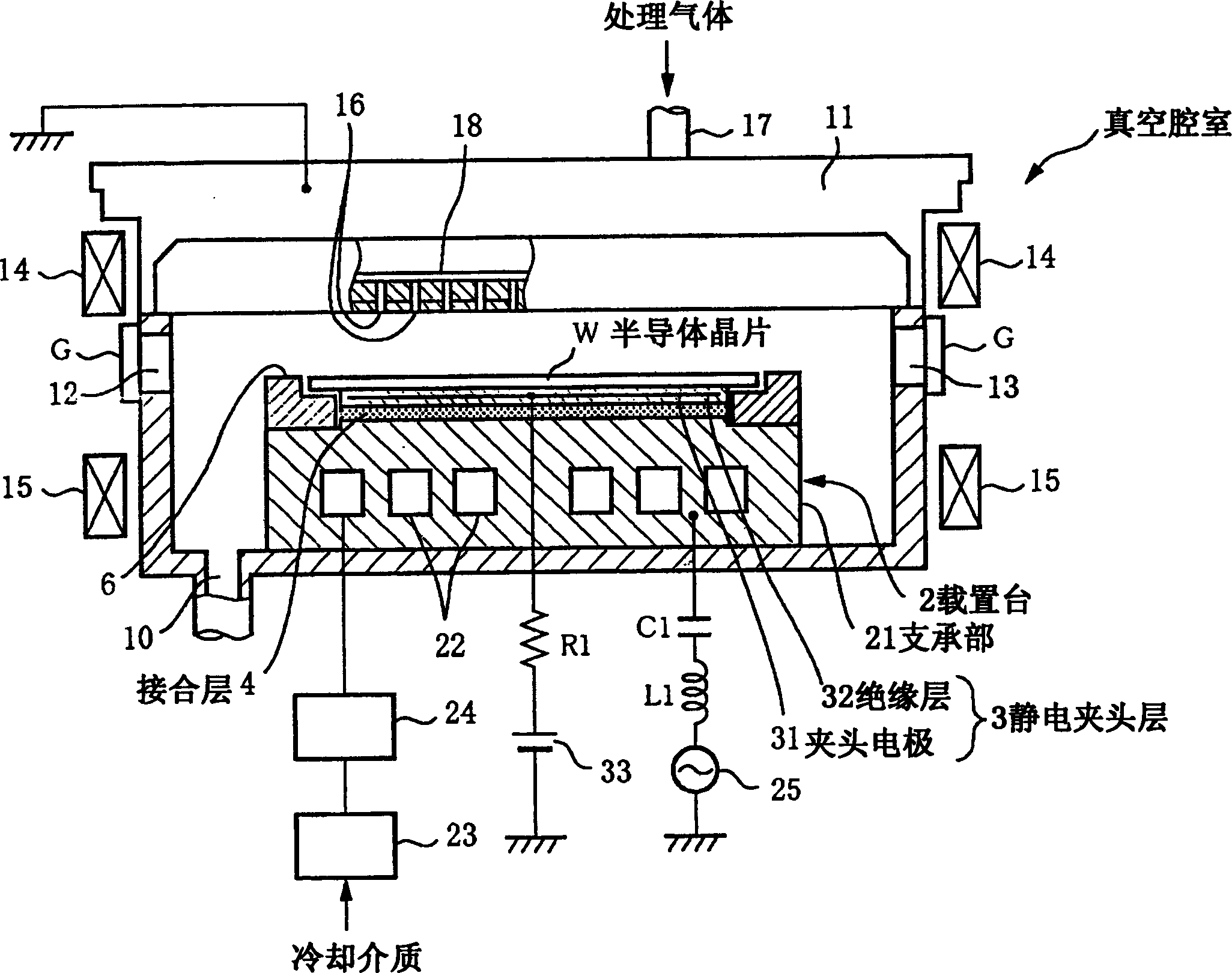
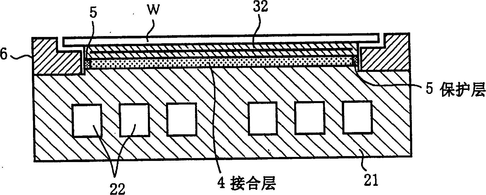
[0060] refer to figure 1 and figure 2 Embodiment 1 of the processing apparatus of the present invention will be described. figure 1 It is a vertical cross-sectional view showing the overall configuration of an example of an etching apparatus as a processing apparatus of this embodiment. 1 in the figure is a vacuum chamber forming a processing container, which may form a sealed structure made of aluminum. In this vacuum chamber 1, an upper electrode 11 serving as a gas shower head (processing gas supply part) and a mounting table 2 serving as a lower electrode are oppositely arranged, and an exhaust port communicating with a vacuum pump not shown in the figure is formed on the bottom surface. 10. Openings 12 and 13 are formed on the side walls of the vacuum chamber 1 for loading and unloading semiconductor substrates such as wafers W which are silicon substrates. The openings 12, 13 can be freely opened and closed by gate valves G, respectively. Ring-shaped permanent mag...

Embodiment approach 2

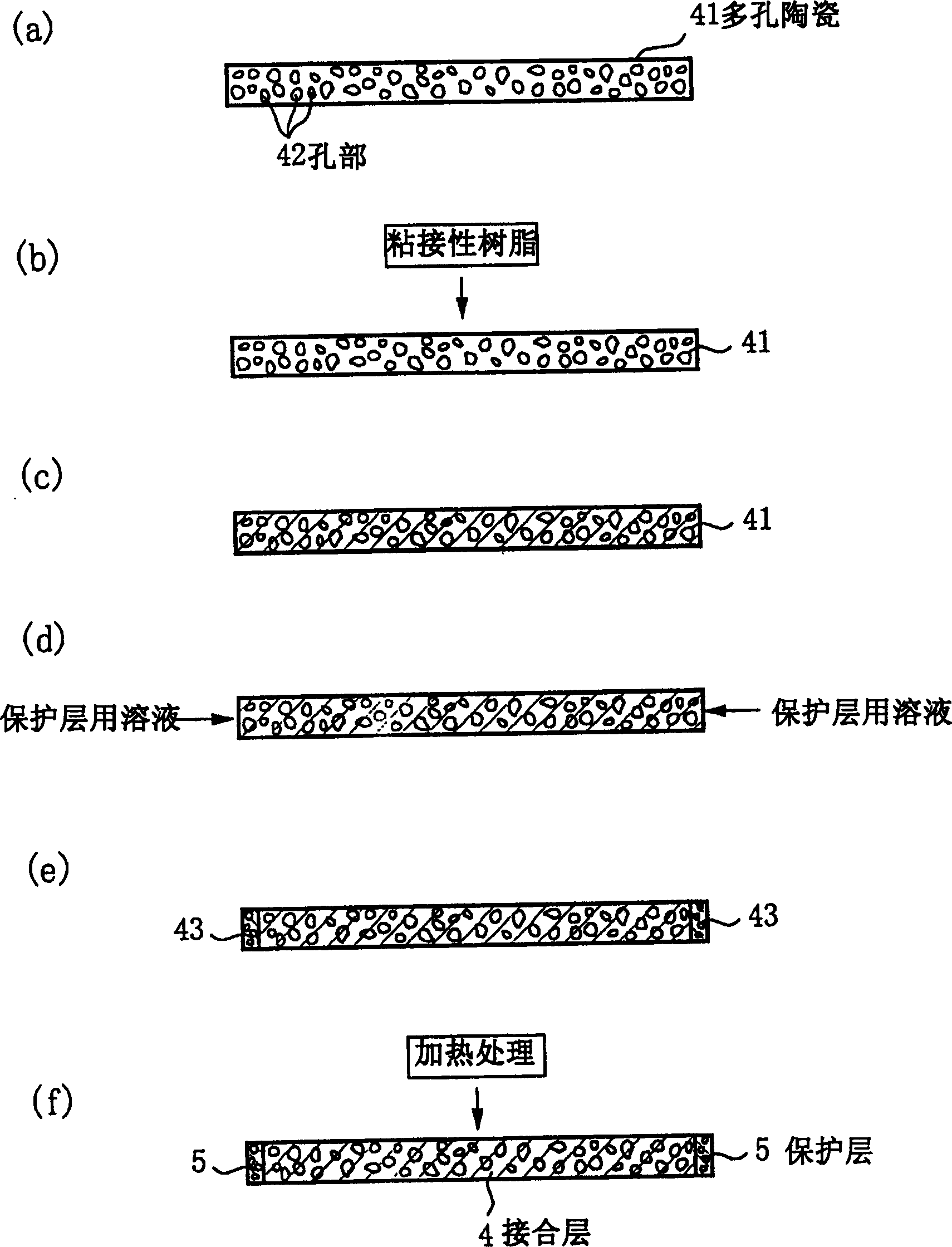
[0089] Another embodiment of the present invention will now be described. Figure 6 It is a figure which shows the mounting table 7 used in this embodiment. The other parts of the processing apparatus (etching apparatus) of this embodiment and figure 1 have the same structure. exist Figure 6 in, with figure 2 The same symbols denote the same part. The bonding layer 70 is used to bond the electrostatic chuck layer 3 and the support portion 21, and may be made of a silicone rubber-based adhesive. In addition, a flexible covering member 71 is provided on the side peripheral surface of the bonding layer 70 to protect the bonding layer 70 from active species such as fluorine radicals or fluorine ions generated by plasma. Another example will be Figure 6 Part of (a) enlarged Figure 6 As shown in (b), a sprayed coating 72 is formed on the central portion of the upper surface of the support table 21 , that is, on the peripheral edge of the convex portion that is a portion ...

Embodiment approach 3

[0104] Embodiment 3 of the processing apparatus of the present invention will now be described. Figure 9 A vertical cross-sectional view showing the entire structure of a plasma apparatus as a processing apparatus for implementing the present invention is used in an etching apparatus. In the figure, 120 is an airtight processing container made of a conductive material such as aluminum, and the processing container 120 is grounded. In this processing chamber 120, an upper electrode 130 serving as a gas shower head serving as a gas supply unit for introducing a predetermined processing gas, and a mounting table 140 serving as a lower electrode on which a wafer W serving as a substrate to be processed is placed are provided facing each other. An exhaust pipe 121 is connected to the bottom of the processing container 120 , and a vacuum exhaust device such as a vacuum pump 122 such as a turbomolecular pump or a dry pump is connected to the exhaust pipe 121 . In addition, a gate v...


PUM

PropertyMeasurementUnit
thicknessaaaaaaaaaa
thermal conductivityaaaaaaaaaa

Abstract

The time period during which a wafer is stabilized to a predetermined temperature by increasing a thermal conductivity of a junction layer for bonding an electrostatic chuck layer and a support together, and the deterioration of the junction layer that is caused by active species generated by plasma is suppressed. Between the electrostatic chuck layer formed by sintering together a chuck electrode made of tungsten and an insulating layer made of alumina and the support, made of aluminum, for supporting the electrostatic chuck layer, the junction layer is provided to bond the electrostatic chuck layer and the support together. The junction layer is formed by impregnating a porous ceramic with a silicone-based adhesive resin. Further, rubber or a heat shrink tube made of a fluoric resin such as PFA is provided as a soft coating member so as to coat a side circumferential surface of the junction layer and the side circumferential surfaces of the electrostatic chuck layer and the support come into a tight contact with the heat shrink tube or rubber.

Description

technical field [0001] The present invention relates to a device for absorbing and holding a substrate on an electrostatic chuck and vacuum processing the substrate. Background technique [0002] In semiconductor device manufacturing processes, substrates are often processed in a vacuum atmosphere, such as film formation by etching or CVD (Chemical Vapor Deposition). Such as Figure 17 As shown, in the vacuum processing apparatus for such processing, in the processing container 9, a mounting table 91 for a semiconductor wafer (hereinafter referred to as a wafer) W serving as a lower electrode is disposed; Gas supply chamber 92 for the upper electrode. A high frequency for generating plasma is applied from the high frequency power supply 91a to the above-mentioned mounting table 91, and plasma is generated between the mounting table 91 and the gas supply chamber 92, and the plasma is introduced from the gas supply chamber 92 into the processing container. The processing gas...

Claims


Application Information

Patent Timeline
Patent Type & Authority Applications(China)
IPC IPC(8): H01L21/00H01L21/683
CPCH01L21/67248H01L21/6833
Inventor 西本伸也樋熊政一武藤慎司藤原尚中山博之岛贯义纪
Owner TOKYO ELECTRON LTD
Why Eureka
Try Eureka