Contact portion of semiconductor device and manufacturing method thereof including thin film transistor array panel for contact portion display device and manufacturing method thereof

A technology of thin-film transistors and semiconductors, which is applied in semiconductor/solid-state device manufacturing, transistors, semiconductor devices, etc., and can solve problems such as uneven organic insulating layers and inconsistent protrusions of reflective films

Inactive Publication Date: 2005-06-01
SAMSUNG DISPLAY CO LTD
View PDF0 Cites 7 Cited by
  • Summary
  • Abstract
  • Description
  • Claims
  • Application Information

AI Technical Summary

Problems solved by technology

[0007] However, the stepped height of the organic insulating layer due to the steep height difference of the underlying structure gives a poor pro

Method used


Image

  • Contact portion of semiconductor device and manufacturing method thereof including thin film transistor array panel for contact portion display device and manufacturing method thereof
  • Contact portion of semiconductor device and manufacturing method thereof including thin film transistor array panel for contact portion display device and manufacturing method thereof
  • Contact portion of semiconductor device and manufacturing method thereof including thin film transistor array panel for contact portion display device and manufacturing method thereof

Examples


Embodiment Construction

[0045] Now, a contact structure of a semiconductor device and a method of manufacturing the same according to an embodiment of the present invention, a TFT array plate including a contact structure and a method of manufacturing the same will be described with reference to the accompanying drawings, so that those skilled in the art can easily implement the present invention.

[0046] First, a method for manufacturing a contact structure of a semiconductor device according to an embodiment of the present invention will be described.

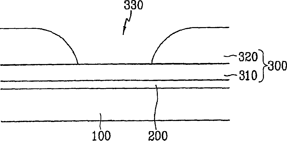
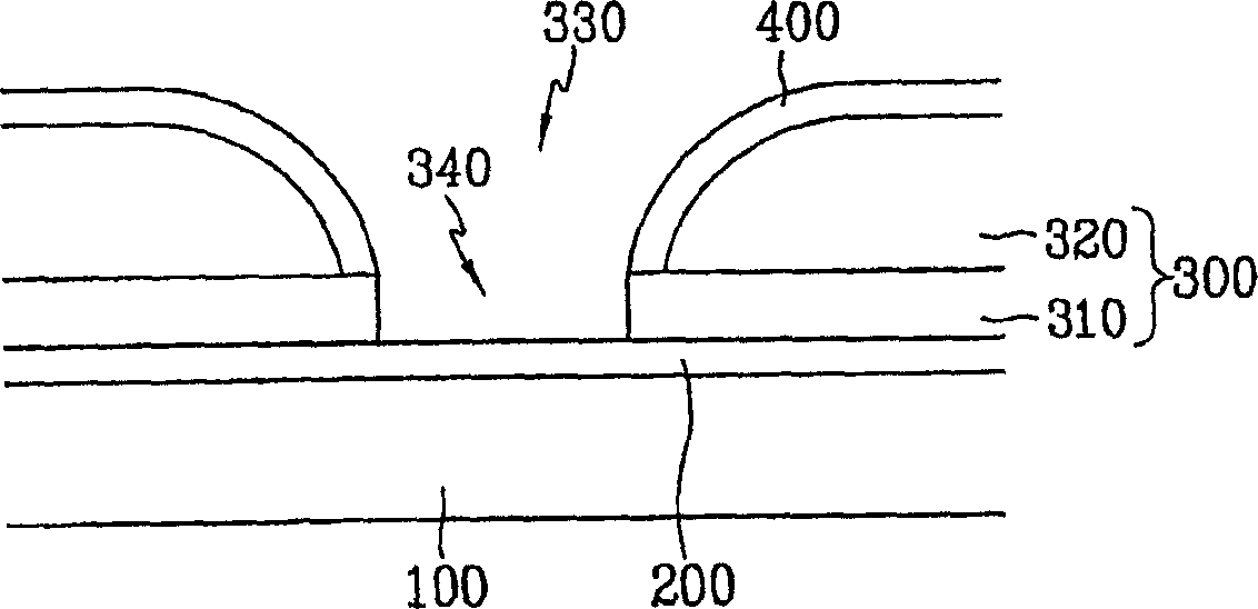
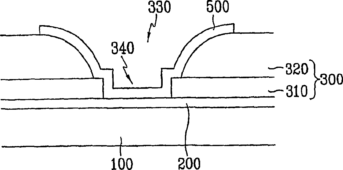
[0047] Generally, a semiconductor device has multilayer wiring interposed between interlayer insulating layers. The interlayer insulating layer is preferably made of a material with a low dielectric constant in order to minimize interference between signals flowing in different wirings, and to electrically connect different wiring layers transmitting the same signal to each other through a contact hole provided at the interlayer insulating layer. c...


PUM

PropertyMeasurementUnit
Widthaaaaaaaaaa

Abstract

A gate wiring including a gate line, a gate electrode and a gate pad and extending in a lateral direction is formed on the substrate. A gate insulating layer is subsequently formed, and a semiconductor layer and an ohmic contact layer are sequentially formed thereon. A conductive material is deposited and patterned to form data wiring including data lines intersecting the gate lines, source electrodes, drain electrodes, and data pads. A first insulating layer made of silicon nitride is deposited on the substrate, and a second insulating layer made of photosensitive organic insulating material is coated on the first insulating layer. The second insulating layer is patterned to form a convex-concave pattern and a first contact hole opposite to the drain electrode exposing the first insulating layer on a surface thereof. Subsequently, the first insulating layer and the gate insulating layer are patterned together by photolithography using a photoresist pattern to form contact holes exposing the drain electrode, the gate pad, and the data pad, respectively. Next, indium tin oxide (ITO) or indium zinc oxide (IZO) is deposited and patterned to form light-transmitting electrodes, sub-gate pads, and sub-gate pads connected to drain electrodes, gate pads, and data pads, respectively. data pad. Finally, a reflective conductive material is deposited on the light-transmitting electrode and patterned to form a reflective film with corresponding holes in the pixel area.

Description

technical field [0001] The invention relates to a contact structure of a semiconductor device and a manufacturing method thereof, a thin film transistor array plate for a display device including a contact structure and a manufacturing method thereof. Background technique [0002] Generally, a semiconductor device has multilayer wiring interposed between interlayer insulating layers. The interlayer insulating layer is preferably made of a material with a low dielectric constant in order to minimize the interference between signals flowing through different wirings, and through the contact hole provided at the interlayer insulating layer, different wiring layers that transmit the same signal are electrically connected to each other. [0003] The interlayer insulating layer includes an organic insulating layer having a low dielectric constant, which is generally formed by spin coating. When the underlying structure of the organic layer has a steep height difference, the orga...

Claims


Application Information

Patent Timeline
IPC IPC(8): H01L29/786G02F1/1335G02F1/1362H01L21/336H01L21/768H01L21/77H01L21/84H01L27/12
CPCG02F1/133555G02F1/136227H01L27/12H01L27/124H01L27/1244H01L27/1248H01L29/66765H01L29/786
Inventor 柳春基
Owner SAMSUNG DISPLAY CO LTD
Why Eureka
Try Eureka