Novel structure Schottky millimeter wave frequency mixing diode

A technology of mixing diodes and millimeter waves, which is applied in the field of microelectronics, can solve the problems of affecting the stability of high-frequency work quality, relying on imports of mixing diodes, and restricting system design to others, so as to improve working performance, small series resistance, and convenient connection Effect

Inactive Publication Date: 2005-06-22
INST OF MICROELECTRONICS CHINESE ACAD OF SCI
View PDF0 Cites 7 Cited by
  • Summary
  • Abstract
  • Description
  • Claims
  • Application Information

AI Technical Summary

Problems solved by technology

In the field of ultra-high frequency communication, the mixing diodes currently used in our country still rely on imports, which leads to our system design being subject to others.
C

Method used


Image

  • Novel structure Schottky millimeter wave frequency mixing diode
  • Novel structure Schottky millimeter wave frequency mixing diode

Examples


Example Embodiment

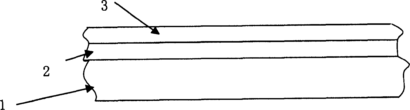
[0036] Epitaxial structure of the present invention sees attached figure 1 . In order to obtain a suitable turn-on voltage and low series resistance, we chose to grow a thick first epitaxial layer 2 of heavily doped gallium arsenide (GaAs) on a semi-insulating gallium arsenide substrate 1 for making ohmic contact electrodes , the doping concentration is generally selected on the order of 10 to the 18th power; a lightly doped gallium arsenide (GaAs) second epitaxial layer 3 suitable for the thickness and impurity concentration required by the process is grown on the upper layer of the first epitaxial layer 2 for making For the Schottky barrier, the doping concentration is generally on the order of 10 to the 16th power. The impurity used for the doping of the two epitaxial layers is silicon.

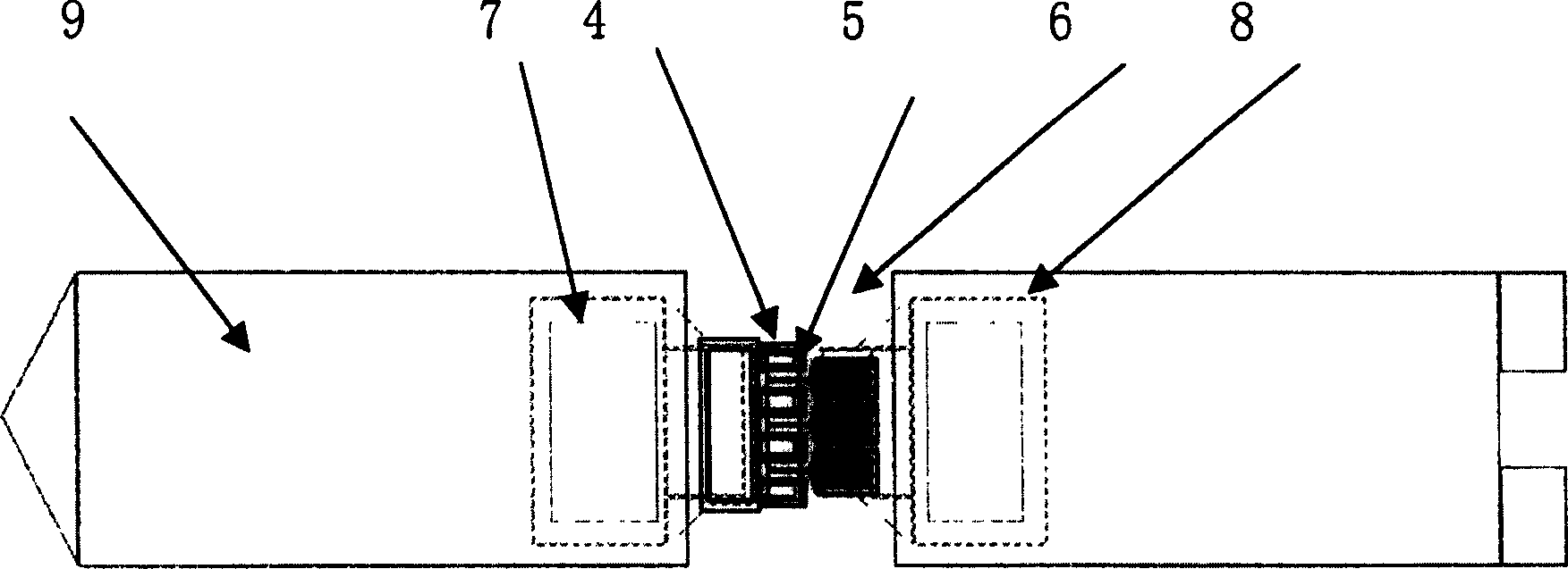
[0037] In terms of device process structure, we choose the electrode width of more than 1 micron, and the lead wire chooses the beam lead method, in order to reduce the series resistance...


PUM


Abstract

This invention refers to a new structured Schottky millimeter wave mixer diode. The chip epitaxy structure is to grow a heavily doped gallium arsenide first epitaxy layer on gallium arsenide substrate and to grow a light doped gallium arsenide second epitaxy layer on the first epitaxy layer. Said invention optimization designs epitaxy structure.

Description

technical field [0001] The invention relates to microelectronic technology, in particular to a high-frequency and high-performance mixing device. Background technique [0002] Frequency mixing is a very critical technology in the field of communication. When the high-frequency signal is in the microwave and millimeter wave bands, Schottky barrier diodes are often used for frequency mixing. The Schottky barrier mixer uses the barrier formed when the metal and the semiconductor are in contact. When it is forward biased, the majority carriers are injected from the semiconductor into the metal, so there is a current flow, and the minority carriers can be ignored in fact. Impact. Compared with pn junction diodes, there is no long reverse recovery time and charge storage capacitance, the slope of the forward I-V curve is steeper, the series resistance is smaller, and the forward turn-on voltage is lower. Especially gallium arsenide (GaAs) Schottky mixer diodes, compared with po...

Claims


Application Information

Patent Timeline
IPC IPC(8): H01L29/872
Inventor 张海英
Owner INST OF MICROELECTRONICS CHINESE ACAD OF SCI
Why Eureka
Try Eureka