Adhesive sheet and semiconductor device and process for producing the same

A thin-film, adhesive technology, used in semiconductor/solid-state device manufacturing, semiconductor devices, adhesive types, etc., to solve problems such as reduced adhesion and low adhesion

Inactive Publication Date: 2005-06-29
HITACHI CHEM CO LTD
View PDF4 Cites 23 Cited by
  • Summary
  • Abstract
  • Description
  • Claims
  • Application Information

AI Technical Summary

Problems solved by technology

In addition, there are problems such as the transfer of the adhesive of the dicing tape to the film-like adhesive and the decrease in adhesion
Therefore, an adhesive sheet having both the functions of a film-like adhesive and a dicing tape is required, but has not yet been obtained with a sufficiently high adhesive force so that the semiconductor element does not fly when dicing, and has a low adhesiveness. Adhesive sheet that meets the opposite requirements so that the components are not damaged during removal

Method used

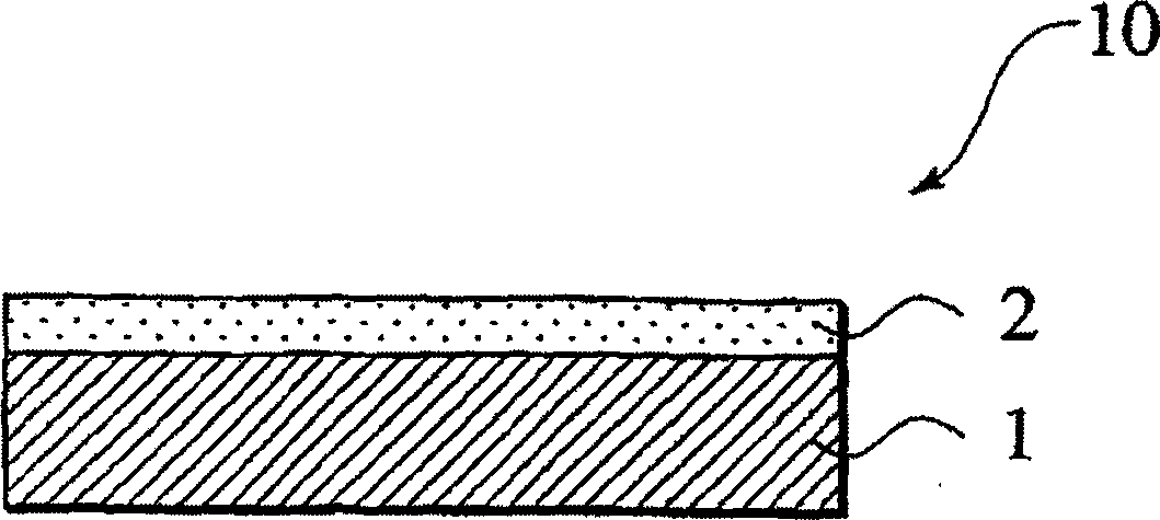
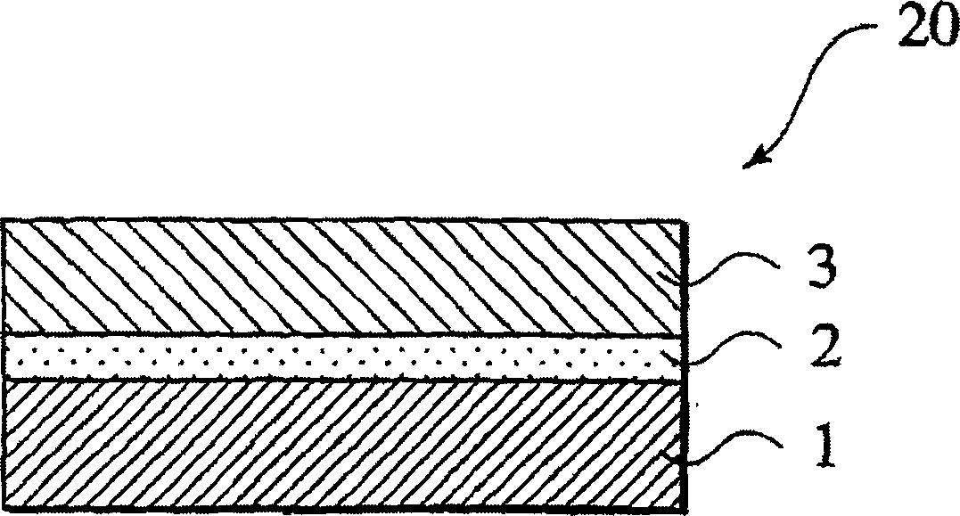
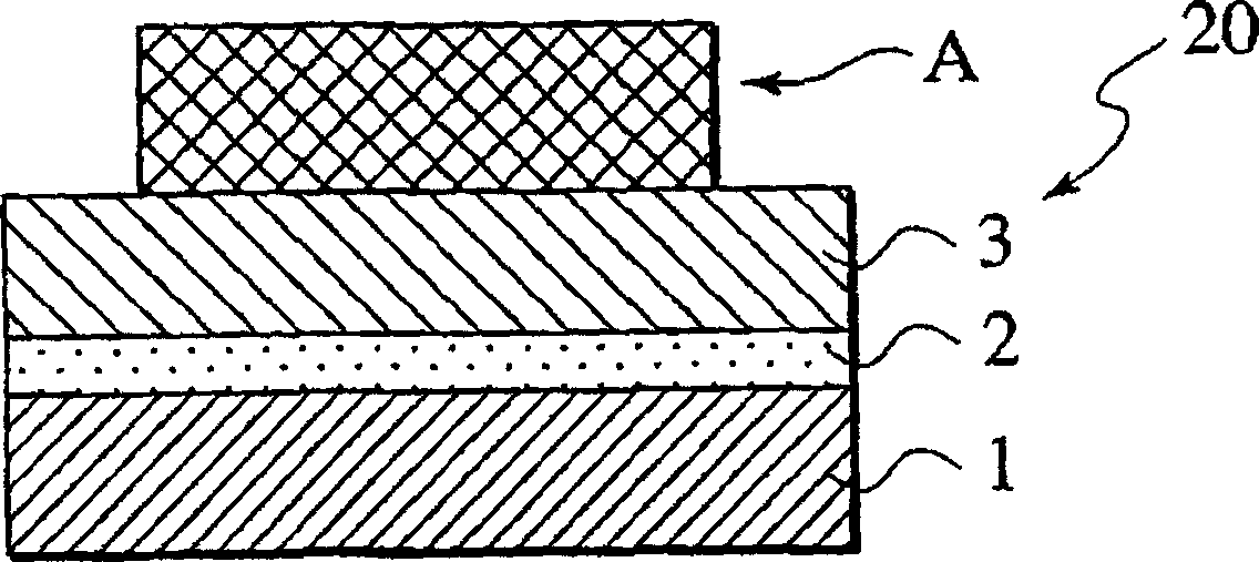

Image

  • Adhesive sheet and semiconductor device and process for producing the same
  • Adhesive sheet and semiconductor device and process for producing the same
  • Adhesive sheet and semiconductor device and process for producing the same

Examples


Embodiment

[0323] Hereinafter, the present invention will be described in more detail using examples. The present invention is not limited by these examples. In addition, the evaluation of the adhesive sheet can be performed according to the method described in the evaluation method column described later, unless otherwise specified in each Example.

Synthetic example 1

[0324] (Synthesis Example 1) [Synthesis of Photobase Generating Agent]

[0325] 30 g of 2-nitrobenzyl alcohol was dissolved in 300 g of tetrahydrofuran by stirring using a magnetic stirrer at room temperature. To this solution, a premixed solution consisting of 24.5 g of 4,4'-diphenylmethane diisocyanate and 100 g of tetrahydrofuran was added dropwise over 30 minutes, and stirred at room temperature for 1 hour. Thereafter, a Liebig cooling tube was attached, and reaction was performed for 2 hours while heating to 60° C. in an oil bath. After the reaction, it was cooled to room temperature, and the reaction solution was concentrated to half using a rotary evaporator.

[0326] Once the obtained concentrate was added to 1000 parts by weight of n-hexane, a white precipitate was obtained. The precipitate was suction-filtered and dried overnight at 60° C. under vacuum to obtain the target product 2-nitrobenzylcarbamate derivative (PB-1). Yield was 49.5 g (91% yield).

Synthetic example 2

[0327] (Synthesis Example 2) [Synthesis of Photobase Generating Agent]

[0328]Add methyl p-nitrobenzoate (2.00g, 11mmol), N,N-dimethylhydrazine (0.66g, 11mmol), phenyl glycidyl ether (1.66, 11mmol) in tert-butanol (15.0g) , after stirring at 50°C for 10 hours, and then stirring at room temperature (25°C) for 48 hours, a white precipitate was formed. The white precipitate was filtered, washed twice with ethyl acetate, and dried with a vacuum dryer to obtain an amine imide compound (PB-2). The yield was 3.67 g, the yield was 85%, and the melting point was 146-147°C.


PUM

PropertyMeasurementUnit
Melting pointaaaaaaaaaa
Storage modulusaaaaaaaaaa

Abstract

An adhesive sheet comprising a pressure-sensitive adhesive layer and a substrate layer, the adhesive force between the pressure-sensitive adhesive layer and the substrate layer is controlled by irradiation with radiation, and the pressure-sensitive adhesive layer contains the following Components: (a) thermoplastic resin, (b) thermopolymerizable component, and (c) a compound that generates a base by irradiation with radiation. The adhesive sheet of the present invention is to have sufficient adhesive force to prevent semiconductor elements from flying away when cutting, and then control the adhesive force between the above-mentioned pressure-sensitive adhesive layer and the substrate by irradiating radiation, so that when taken out Such an oppositely required adhesive sheet with low adhesion that does not damage the components.

Description

technical field [0001] The present invention relates to an adhesive sheet, a semiconductor device using the adhesive sheet, and a manufacturing method thereof. Background technique [0002] Conventionally, a silver paste has been mainly used for joining a semiconductor element and a supporting member for mounting a semiconductor element. However, along with the miniaturization and high performance of semiconductor elements in recent years, the supporting members used are also required to be miniaturized and finer. For such requirements, due to the occurrence of defects in wire bonding due to overflow or inclination of semiconductor elements, difficulty in controlling the film thickness of the adhesive layer, and the occurrence of voids in the adhesive layer, etc., silver paste has not been able to Meet the above requirements. [0003] Therefore, in order to meet the above-mentioned requirements, film-like adhesives have been used in recent years. [0004] This film-like a...

Claims


Application Information

Patent Timeline
IPC IPC(8): C09J7/22C09J7/38C09J163/00H01L21/68
CPCC09J163/00C09J2203/326C09J2463/00H01L21/6836H01L2221/68327H01L2924/30105H01L24/27H01L24/29H01L24/83H01L2224/83191H01L2924/01012H01L2924/01029H01L2224/83H01L2924/351C09J7/38C09J7/22H01L2924/3512H01L2924/00
Inventor 川上广幸稻田祯一增子崇大久保惠介畠山惠一柳川俊之加藤木茂树
Owner HITACHI CHEM CO LTD
Why Eureka
Try Eureka