Method for preparing film specimen in use for transmission electron microscope
A technology for transmission electron microscopy and samples, which is applied in the preparation of test samples, sputtering plating, ion implantation plating, etc., can solve the problems that thin film samples for electron microscopy are easy to be polluted, broken, and introduce artifacts, etc., and achieve low working temperature , Strong adhesion, good peeling effect
- Summary
- Abstract
- Description
- Claims
- Application Information
AI Technical Summary
Problems solved by technology
Method used
Image
Examples
Embodiment 1
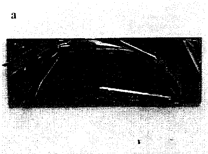
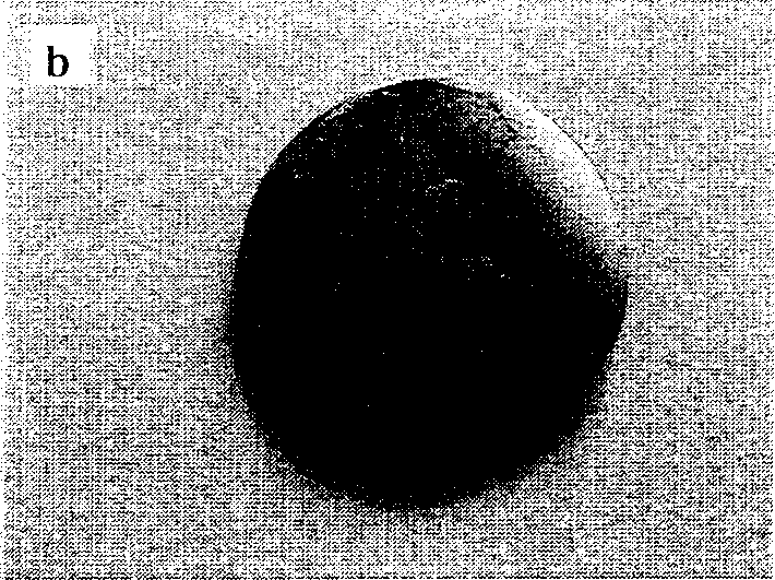
[0039] Sample preparation: Put the glass and Mo slices that have been ultrasonically cleaned and degreasing with acetone and alcohol as substrates in soapy water, soak for 2 minutes, then take out and air-dry, so that the surface is evenly coated with a layer of soap film; then use TiZrYAl The alloy target is the negative electrode, and the glass substrate and the Mo substrate are respectively used as the positive electrode. The magnetron sputtering coating machine adopts the following process parameters to prepare: vacuum first during sputtering until the background vacuum reaches 6.0×10 -5 Pa, and then pass in Ar gas with a purity of 99.99% to maintain the vacuum degree during coating at 7.0×10 -1 About Pa, current 1A, voltage 160V, sputter coating on the substrate after 5 minutes of pre-sputtering, the coating time is 90 minutes, and the film thickness is about 9μm. Figure 1a with Figure 1b The photos of the glass substrate and the Ti alloy film of Mo obtained after sputterin...
Embodiment 2
[0042] The difference from Example 1 is:
[0043] Sample preparation: Place the monocrystalline Si wafer as a substrate in soapy water after ultrasonic cleaning and degreasing with acetone and alcohol, soak for 4 minutes, and then take it out to air dry so that its surface is evenly coated with a layer of soap film; then use Fe alloy target (Alloy brand: FeZrSiMn) is the negative electrode, and the single crystal Si wafer is the positive electrode. The following process parameters are used on the magnetron sputtering coating machine. During sputtering, vacuum is first drawn until the background vacuum reaches 3.0×10 -5 Pa around, and then pass in Ar gas with a purity of 99.99% to maintain the vacuum at 6.5×10 during coating -1 About Pa, current 1A, voltage 200V, sputter coating on the substrate after 2 minutes of pre-sputtering, the coating time is 60 minutes, and the film thickness is about 5μm. Figure 2a It is a photo of the Fe alloy film of the silicon substrate obtained after...
Embodiment 3
[0046] The difference from Example 1 is:
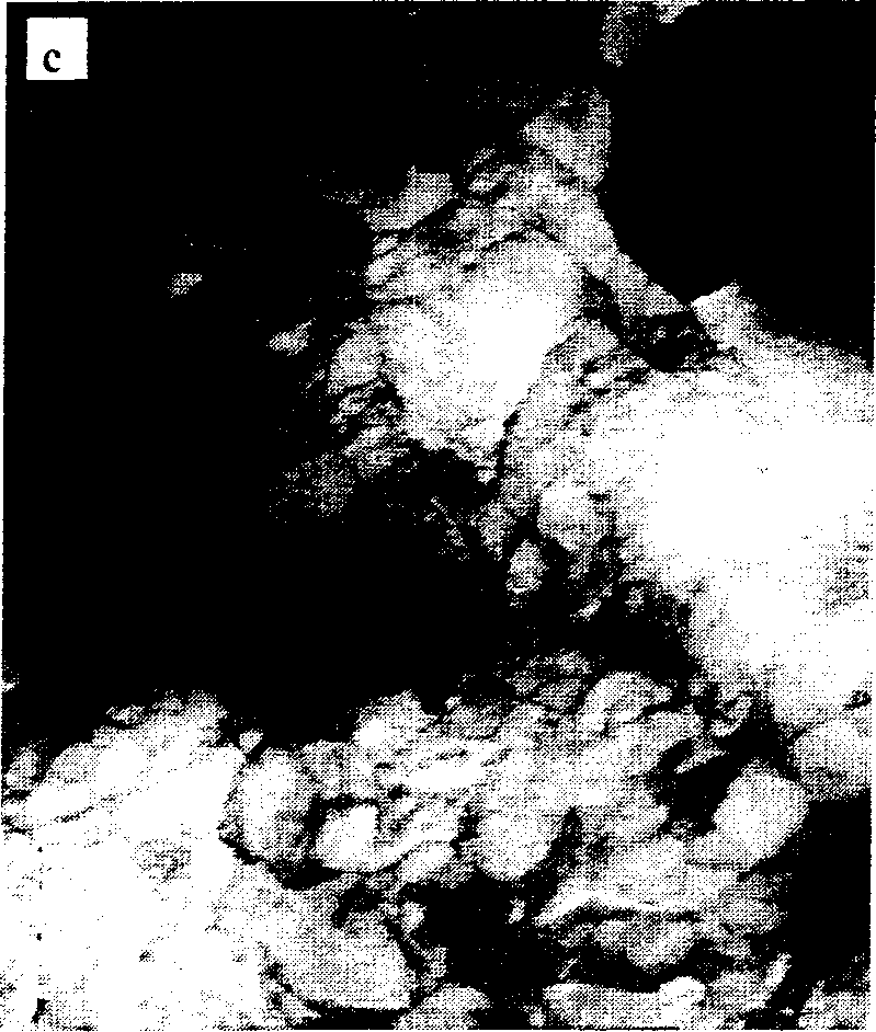
[0047]Sample preparation: Put the stainless steel that has been ultrasonically cleaned and degreasing with acetone and alcohol as a substrate in soapy water, soak for 4 minutes, and then take it out to air dry so that its surface is evenly coated with a layer of soap film; then use Ti (purity of 99.9 %) The target is the negative electrode and the stainless steel sheet is the positive electrode. The following process parameters are used on the magnetron sputtering coating machine. During sputtering, vacuum is first drawn until the background vacuum reaches 8.0×10 -5 Pa around, and then pass in Ar gas with a purity of 99.99% to maintain the vacuum during coating at 6.8×10 -1 About Pa, current 1A, voltage 180V, sputter coating on the substrate after 3 minutes of pre-sputtering, the coating time is 80 minutes, and the film thickness is about 8μm. Figure 3a This is a photo of the Ti film of the stainless steel substrate after sputtering. It ...
PUM
| Property | Measurement | Unit |
|---|---|---|
| thickness | aaaaa | aaaaa |
| diameter | aaaaa | aaaaa |
Abstract
Description
Claims
Application Information


