
Batch spherical semiconductor grain producing equipment and method

A mass production and semiconductor technology, applied in the direction of semiconductor devices, crystal growth, chemical instruments and methods, etc., can solve the problem of poor cost reduction

Inactive Publication Date: 2005-12-14
CLEAN VENTURE 21
View PDF2 Cites 6 Cited by
  • Summary
  • Abstract
  • Description
  • Claims
  • Application Information

AI Technical Summary

Problems solved by technology

[0011] This prior art requires much time and labor to manufacture spherical semiconductor particles, and thus is inferior in cost reduction

Method used


Image

  • Batch spherical semiconductor grain producing equipment and method
  • Batch spherical semiconductor grain producing equipment and method
  • Batch spherical semiconductor grain producing equipment and method

Examples


example 1

[0218] About 1.5 ml of silicon material was added to a graphite crucible. The graphite crucible has an outer diameter of 20 mm, an outer length of 40 mm, its volume is represented by an inner diameter of 10 mm and a length of 35 mm, and is accommodated in a ceramic airtight and thermally insulated container with a nozzle at one end of the container having an inner diameter of 1 mm and a length of 5 mm. Immediately before particle production, 4.6kW of high-frequency induction power was applied for about 20 minutes to stabilize particle production conditions such as temperature. Particle formation was started by applying a nitrogen pressure of about 300 Pa, resulting in silicon spheres having an average diameter of about 1 mm. In order to reduce the degree of reaction between silicon and graphite and the degree of combustion of graphite due to the presence of oxygen, a nitrogen pressure of about 100 Pa is maintained in the system where the flow rate becomes zero at the beginning...

example 2

[0220] About 1.5 ml of silicon material was added to a graphite crucible. The graphite crucible has an outer diameter of 20 mm, an outer length of 40 mm, its volume is represented by an inner diameter of 10 mm and a length of 30 mm, and is accommodated in a ceramic airtight and heat-insulated container with a nozzle of an inner diameter of 1 mm and a length of 10 mm at one end of the container. Immediately before particle production, 4.6kW of high-frequency induction power was applied for about 15 minutes to stabilize particle production conditions such as temperature. Particle formation was started by applying a nitrogen pressure of about 500 Pa, resulting in silicon spheres having an average diameter of about 1 mm. In order to reduce the degree of reaction between silicon and graphite and the degree of combustion of graphite due to the presence of oxygen, a nitrogen pressure of about 100 Pa is maintained in the system where the flow rate becomes zero at the beginning of appl...

example 3

[0222] About 1.2 ml of silicon material was added to a graphite crucible. The graphite crucible has an outer diameter of 20 mm, an outer length of 40 mm, its volume is represented by an inner diameter of 10 mm and a length of 25 mm, and is accommodated in a ceramic airtight and heat-insulated container with a nozzle of an inner diameter of 1 mm and a length of 10 mm at one end of the container. Immediately before particle production, a high-frequency induction power of 3.6kW was applied for about 20 minutes to stabilize particle production conditions such as temperature. Particle formation was started by applying a nitrogen pressure of about 300 Pa, resulting in silicon spheres having an average diameter of about 1 mm. In order to reduce the degree of reaction between silicon and graphite and the degree of combustion of graphite due to the presence of oxygen, a nitrogen pressure of about 100 Pa is maintained in the system where the flow rate becomes zero at the beginning of ap...


PUM

PropertyMeasurementUnit
thicknessaaaaaaaaaa
thicknessaaaaaaaaaa
angleaaaaaaaaaa

Abstract

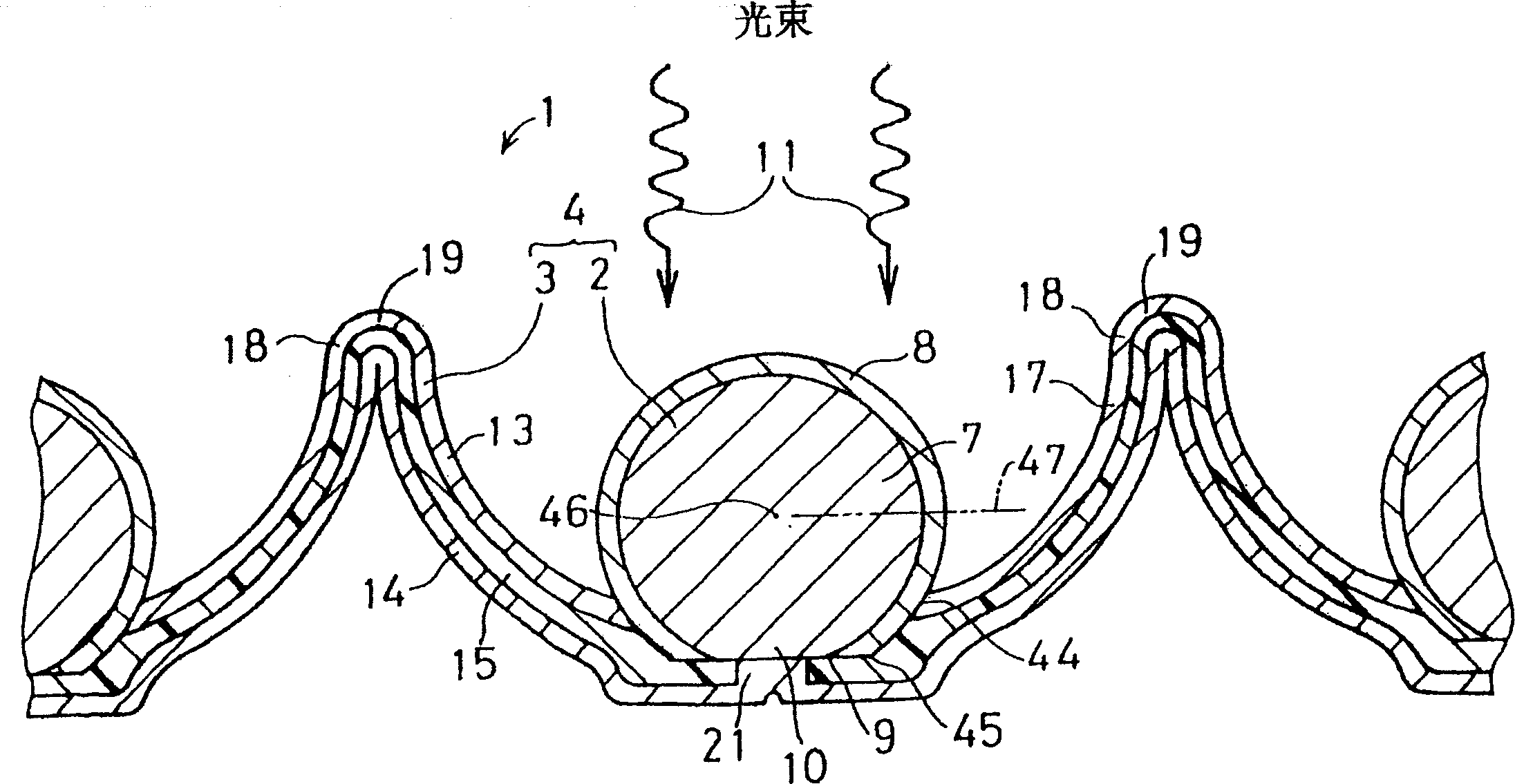
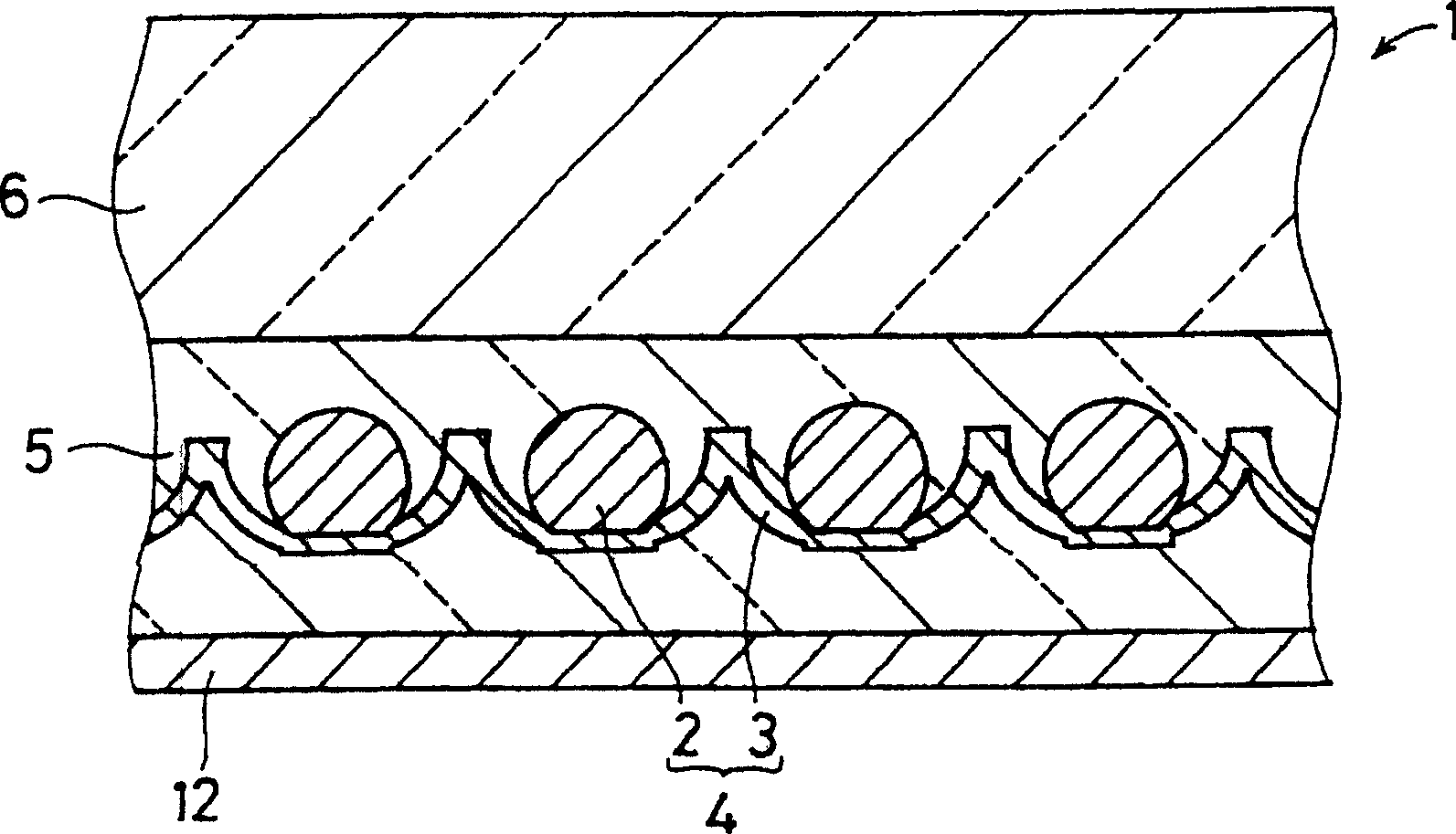
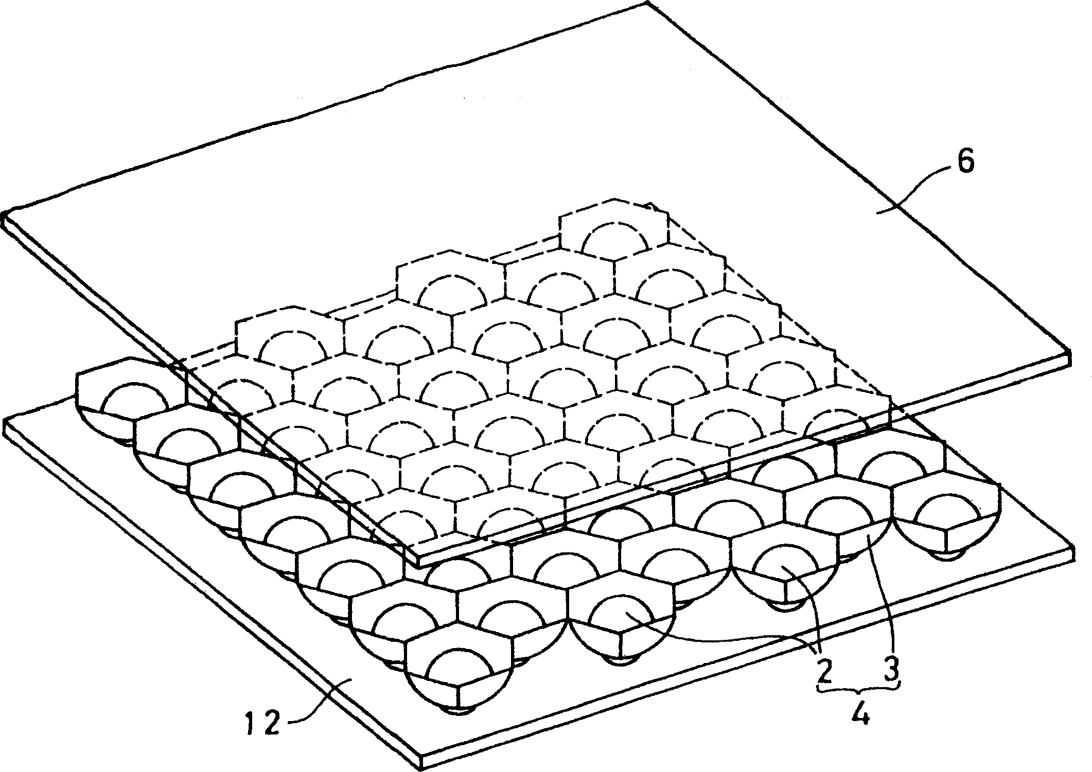
PROBLEM TO BE SOLVED: To provide a photovoltaic device at low cost by reducing the consumption of high purity Si material. SOLUTION: Photoelectric conversion elements 2 are mounted in a plurality of recesses 17 formed on a support 3, respectively, and reflected light inside the recesses 17 is cast to the photoelectric conversion element 2. The photoelectric conversion element is almost spherical, and a p-type amorphous SiC (abbreviated a-SiC) layer 8 with an optical band gap wider than an n-type amorphous Si (abbreviated a-Si) is applied to the outer side of the n-type a-Si layer 7 on the center side. Then a p-n junction is formed. A first conductor 13 of the support is connected with the p-type a-SiC layer 8 of the photoelectric conversion element at the bottom of a recess or the nearby place thereof. A second conductor 14 through an electrical insulator 15 of the support is connected with the n-type a-Si layer 7 of the photoelectric conversion element.

Description

technical field [0001] The present invention relates to a photoelectric device, and a mass production method and device for mass-producing spherical semiconductor particles suitable for manufacturing photoelectric devices and the like. [0002] In the disclosure described herein, the term "pin junction" should be understood to include a structure in which n-, i-, and p-type semiconductor layers are formed on an approximately spherical photoelectric conversion element, and thereby these semiconductor layers are The order is set outward from the inside of the approximately spherical photoelectric conversion element or set inward from the outside. Background technique [0003] A typical prior art provides a photoelectric device comprising a photoelectric conversion element made of a crystalline silicon semiconductor wafer. The optoelectronic devices of the prior art are costly due to the complicated crystal fabrication steps. In addition, the steps of making semiconductor waf...

Claims


Application Information

Patent Timeline
Patent Type & Authority Applications(China)
IPC IPC(8): H01L31/04C30B13/00
CPCY02E10/52Y02E10/545Y02E10/548
Inventor 浜川圭弘室园干男高仓秀行山口由岐夫山形顺安田英典
Owner CLEAN VENTURE 21
Learn More