Epitaxial growing lanthanum aluminate film material on silicon substrate and preparation method
A technology of epitaxial growth and thin film materials, which is applied in the directions of single crystal growth, crystal growth, single crystal growth, etc., can solve the problems of uneven interface reaction layer and oxide film, achieve a wide range of applications and application value, and the process is simple and low , low cost effect
- Summary
- Abstract
- Description
- Claims
- Application Information
AI Technical Summary
Problems solved by technology
Method used
Image
Examples
Embodiment 1
[0036] Use conventional laser molecular beam epitaxy equipment to epitaxially grow 500nm thick LaAlO on n-type silicon wafers 3 Thin film, the present invention is described in detail below in conjunction with preparation method:
[0037] The LaAlO of this embodiment 3 The specific preparation process of the film is:
[0038] 1. Choose a no-clean 2-inch single-side polished n-type single crystal Si substrate;
[0039] 2. Use single crystal LaAlO 3 make target;
[0040] 3. After rinsing in 1% hydrofluoric acid washing solution for 10 seconds, directly put the silicon wafer into the epitaxial chamber;
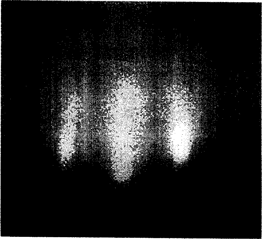
[0041] 4. Vacuum the epitaxial chamber to 2×10 -5 Pa, ~5 cell layers (~150 laser pulses) of LaAlO sputtered on a Si substrate using an excimer laser with an output energy of 250 mJ 3 thin film, the temperature of the silicon wafer was raised to 620°C in 10 minutes, and the LaAlO 3 The crystallization of the film, after the RHEED diffraction fringes appear (such as figure...
Embodiment 2
[0046] Make according to embodiment 1, prepare the LaAlO of 400nm 3 film. The difference from Example 1 is that a high-temperature sintered lanthanum aluminate target is used instead of a single crystal lanthanum aluminate target, a p-type silicon substrate is selected, and 3×10 -1 Pa reactive oxygen species to prepare 400nm LaAlO 3 film.
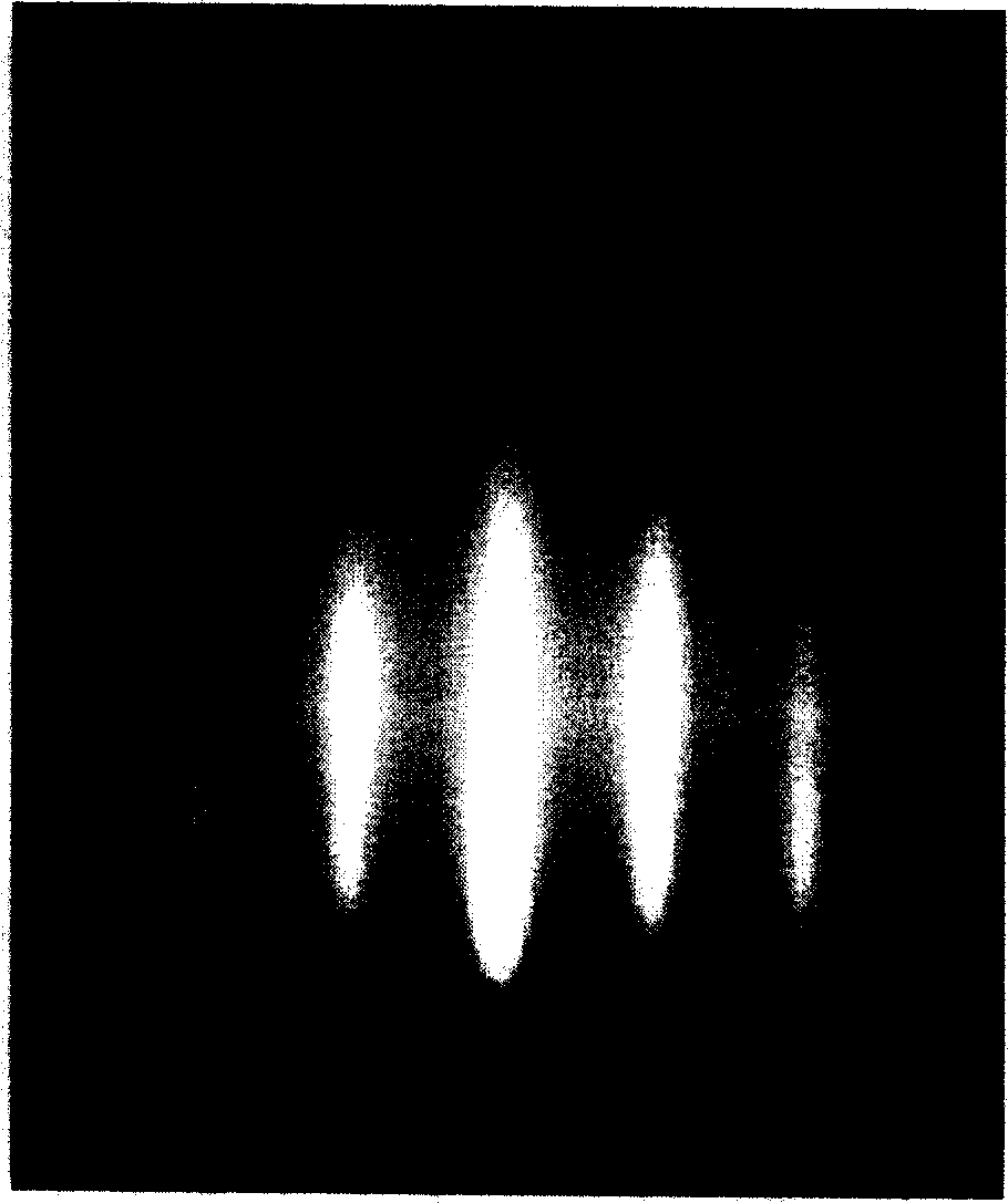
[0047] figure 2 For the epitaxial growth of 400nm thick LaAlO on p-type Si substrate 3 RHEED diffraction fringes of thin films, sharp and clear diffraction fringes, indicating the epitaxial growth of LaAlO on p-type Si substrate 3 The film not only has good crystallinity, but also has a smooth surface.
Embodiment 3
[0049] With conventional laser molecular beam epitaxy equipment, the LaAlO 3 The thin film is used as a buffer layer, and 800nm thick La is epitaxially grown on the n-type silicon wafer 0.7 Sr 0.3 MnO 3 film.
[0050] Using laser molecular beam epitaxy, select a no-clean 4-inch single-side polished n-type single crystal Si substrate, rinse it in 1% hydrofluoric acid for 20 seconds, and then directly put the silicon wafer into the epitaxial chamber, put the epitaxial chamber Vacuum down to 2 x 10 -5 Pa, LaAlO sputtered with ~10 cell layers (~300 laser pulses) on Si substrate 3 thin film, the temperature of the silicon wafer was raised to 680°C in 10 minutes, and LaAlO was observed with RHEED 3 The crystallization of the film, after the RHFFD diffraction fringes appear (such as figure 1 shown), the LaAlO 3 Thin film is used as a buffer layer, and La 0.7 Sr 0.3 MnO 3 The target starts continuous laser sputtering epitaxial growth with a pulsed laser frequency of 2 Hz ...
PUM
| Property | Measurement | Unit |
|---|---|---|
| thickness | aaaaa | aaaaa |
| thickness | aaaaa | aaaaa |
| surface roughness | aaaaa | aaaaa |
Abstract
Description
Claims
Application Information


