
Method for preparing polysilicon

A polysilicon and amorphous silicon thin film technology, applied in semiconductor/solid state device manufacturing, electrical components, circuits, etc., can solve the problems of reducing on-state current and device stability, low hydrogen content of polysilicon thin film, and small grain size, etc. Achieve the effect of shortening the crystallization cycle and reducing the substrate temperature

Inactive Publication Date: 2006-02-01
CHANGCHUN INST OF OPTICS FINE MECHANICS & PHYSICS CHINESE ACAD OF SCI
View PDF0 Cites 6 Cited by
  • Summary
  • Abstract
  • Description
  • Claims
  • Application Information

AI Technical Summary

Problems solved by technology

This method catalyst will contaminate the deposited polysilicon film, this problem has not been solved
[0005] Laser crystallization (ELA) technology is relatively mature and has been widely used in Japan and South Korea. This method is a melting and recrystallization process of amorphous silicon, and the crystallization time is short. The obtained polysilicon film has low hydrogen content and is relatively dense, but the crystal grains are small. , The large area is not uniform enough, which reduces the on-state current and the stability of the device
[0006] The polysilicon film prepared by the metal induction method (MIC / MILC / MIUC) has good uniformity and can be applied in a large area; in order to reduce the pollution of metal ions in the channel region of the device, the lateral induction method is adopted; but the disadvantage of the lateral induction is that there are crystals in the channel region. Boundary barrier, the improved method is unilateral lateral induction to move the grain boundary out of the channel; the metal induction method to prepare polysilicon film has a long period (several to tens of hours)

Method used


Image

  • Method for preparing polysilicon

Examples


Embodiment

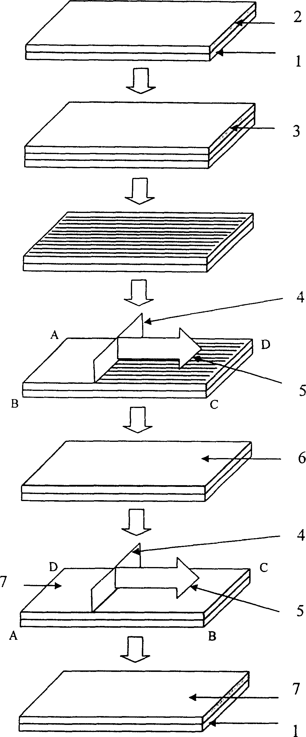
[0023] A 50nm-thick amorphous silicon film (a-Si) 2 was deposited on a common glass substrate 1 by plasma enhanced chemical vapor deposition (PECVD), the substrate temperature was 220°C, and the radio frequency power density was 0.03W / cm 2 , the gas flow rate is 15 sccm, and the reaction chamber pressure is 80Pa.

[0024] The above-mentioned amorphous silicon sample is placed in a magnetron sputtering table to sputter a 5nm metal nickel film 3, the substrate temperature is 150°C, and the radio frequency power density is 0.03W / cm 2 , the background vacuum is 2×10 -4 Pa.

[0025] The metal nickel thin film 3 is photoetched into a line shape with a width of 2 μm and a pitch of 4 μm using ultraviolet lithography technology.

[0026] Use a XeCl (308nm) laser annealing system to perform a laser annealing on the sample at room temperature, make the laser knife 4 perpendicular to the nickel line, place the sample in the laser knife scanning direction 5 parallel to the nickel line, a...


PUM


Abstract

A process for preparing polycrystal silicon includes preparing non-crystal silicon film on glass substrate, preparing a thin Ni layer, photoetching the Ni layer to become fine lines, laser annealing, removing excessive Ni, and laser annealing again for crystallizing the silicon film. Its advantages are short time and low substrate temp.

Description

technical field [0001] The invention belongs to the technical field of semiconductor materials and relates to a silicon material, specifically a method for converting amorphous silicon into polycrystalline silicon. Background technique [0002] Compared with amorphous silicon, the carrier mobility of polysilicon increases by two orders of magnitude, so it is widely used in the production of thin-film transistors in flat panel displays and even in the production of driving ICs. [0003] The preparation method of polysilicon is divided into high temperature preparation and low temperature preparation according to the preparation temperature. High temperature preparation is not suitable for cheap glass or plastic substrates. Therefore, how to prepare high-quality polysilicon thin films at low temperature has become a research hotspot at home and abroad. At present, the main methods for preparing polysilicon thin films at low temperature are: catalyst pre-deposition method (Cat-...

Claims


Application Information

Patent Timeline
IPC IPC(8): C30B29/06H01L21/34
Inventor 黄金英付国柱荆海凌志华
Owner CHANGCHUN INST OF OPTICS FINE MECHANICS & PHYSICS CHINESE ACAD OF SCI
Learn More