Heteroepitaxy method for GaN semiconductor material

A heterogeneous epitaxy and semiconductor technology, applied in the field of microelectronics, can solve the problems of high cost, pollution in the etching process, long process cycle, etc., and achieve extended service life, simple template deposition and etching process, and increased storage capacity. The effect of capacity

Inactive Publication Date: 2006-02-22
XIDIAN UNIV
View PDF0 Cites 14 Cited by
  • Summary
  • Abstract
  • Description
  • Claims
  • Application Information

AI Technical Summary

Problems solved by technology

[0016] The purpose of the present invention is mainly to solve the problems of long process cycle, high cost and serious pollution in the etching process of the above-mentioned prior art, and to provide a heterogeneous epitaxy method for preparing high-quality and large-area GaN-based semiconductor thin films with PE technology, so as to achieve Upgrading of LEO and PE processes to improve the quality of final products

Method used


Image

  • Heteroepitaxy method for GaN semiconductor material
  • Heteroepitaxy method for GaN semiconductor material
  • Heteroepitaxy method for GaN semiconductor material

Examples


Embodiment 1

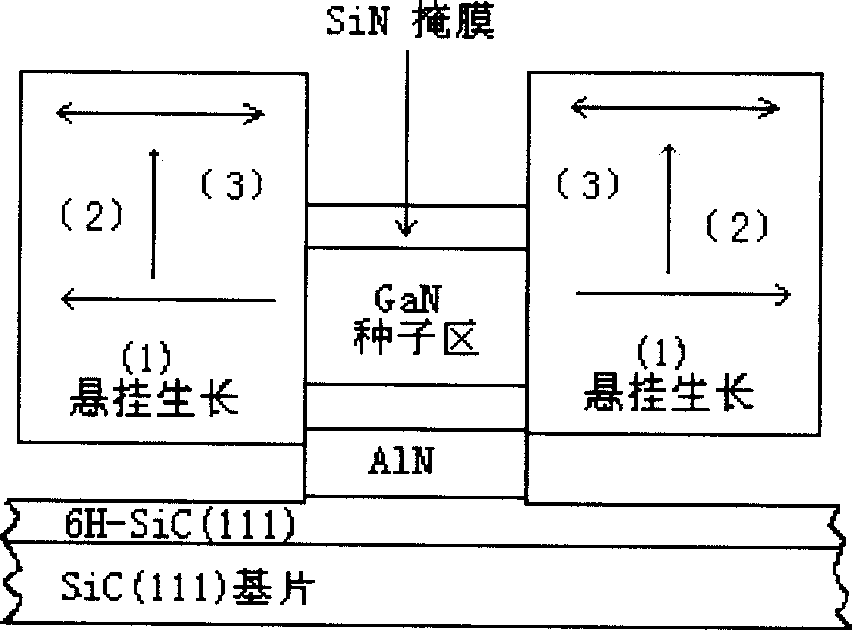
[0035] The substrate SiC (111) is selected as the growth substrate, and the GaN density film is prepared according to the following process:

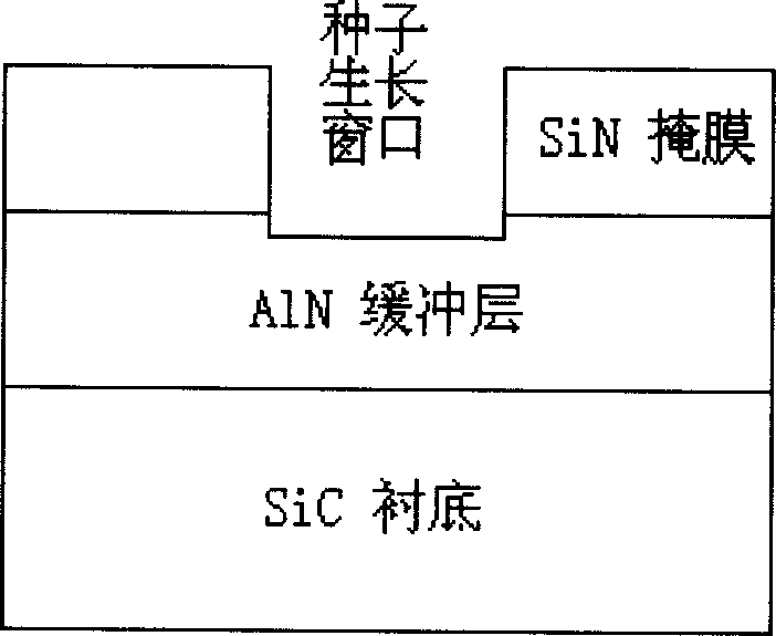
[0036] a. Template preparation

[0037] SiC (111) wafers with a diameter of 1 inch were ultrasonically cleaned in buffer HF for 1 min before growth; rinsed with deionized water and dried, placed in the reaction chamber, and introduced SiH at a suitable high temperature 4 、H 2 mixture, where SiH 4 Accounting for 5%, a 6H-SiC(111) transition film with a thickness of about 1 μm is deposited on the SiC(111) substrate. Next, an AlN buffer layer with a thickness of about 100nm and a SiN thin film are deposited sequentially on the transition layer as a mask, and finally a nickel film is deposited.

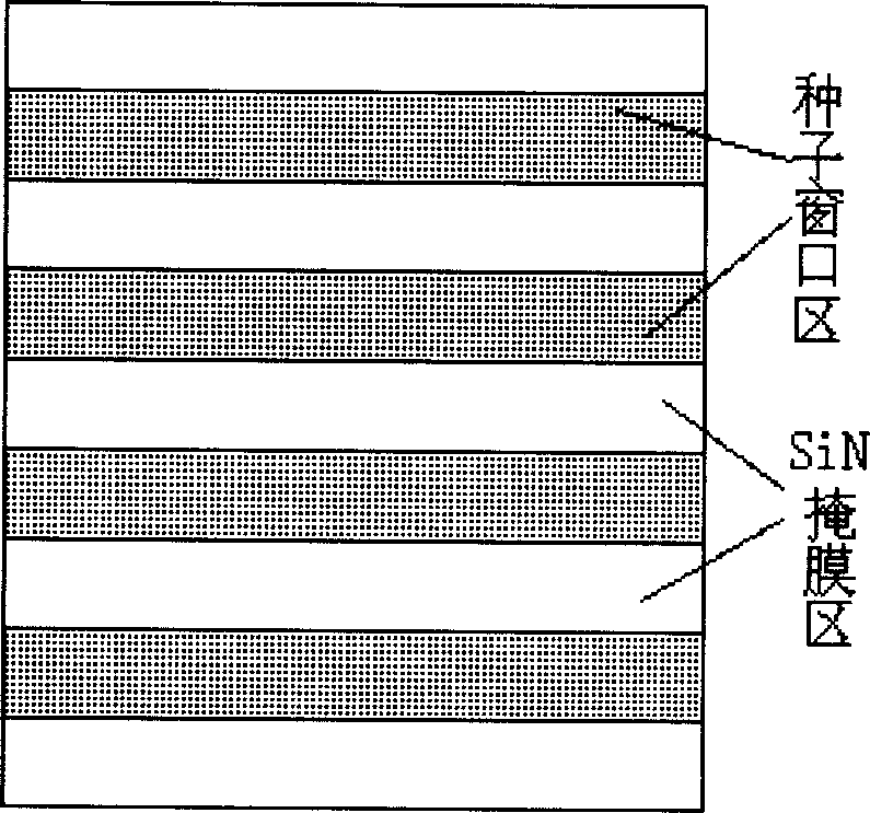
[0038] Using standard photolithography techniques, the reactive sputtering method follows image 3 The bar spacer template flat pattern shown or Figure 4 Part of the nickel film is removed from the planar pattern of the regular hexagonal arra...

Embodiment 2

[0047] The choice of growth substrate sapphire (Al 2 o 3 ) and single crystal silicon, the process of preparing a low defect density GaN thin film is basically the same as that of Example 1.

[0048] The main difference is that in the preparation of the template, before depositing a 6H-SiC(111) transition film with a thickness of about 1 μm, the sapphire Al 2 o 3 A layer of amorphous SiC is deposited on the (111) polished surface of single crystal silicon. The deposition of amorphous SiC is characterized by low substrate temperature and high concentration of precursor gas, and the deposition thickness is about 100nm. Subsequent processes basically follow the steps and parameters of Example 1 to complete the preparation of high-quality thin films.


PUM


Abstract

The invention discloses a heterogeneous epitaxial method of GaN semi-conducting material. First, utilizing the technology of metallorganics chemical vapor deposition, deposing the buffer layer and mask on the surface of SiC substrate (111) and sapphire substrate (0001), etching the mask according the relative pattern, entering and exposing the buffer layer AlN as the area for growing seeds; then, arranging the growing temperature of said area in 1050~110 Deg. C, the pressure beside 40tor, and the seeds in the type of stone can be attained on the buffer layer AlN to grow epitaxially in the form of pyramid, growing mainly in the longitudinal vertical direction while crosswise slow; when reaching the correct height in the vertical direction, changing the growth processing parameters to enter the coronal growing process which covering the upper part of SiN mask by net, as crosswise growing mainly while the vertical growing is slow. The invention has the advantages of simple processing, high performance of film, and the application to the preparation of low defect concentration semi-conducting film material.

Description

technical field [0001] The invention belongs to the technical field of microelectronics, and relates to a preparation method of a semiconductor film material with a low defect density, in particular to a heterogeneous epitaxy method of GaN semiconductor series materials. Background technique [0002] With the development of modern weaponry and aerospace, nuclear energy, and communication technologies, higher requirements are placed on the performance of semiconductor devices. SiC and GaN are representative devices of the third-generation wide bandgap semiconductors. GaN series materials have the characteristics of large bandgap width, high electron saturation drift speed, small dielectric constant, and good thermal conductivity. They can be used to make high temperature, high frequency and large power electronics. However, the GaN series materials grown by traditional methods have the disadvantages of high defect density, large leakage current and short service life of the ...

Claims


Application Information

Patent Timeline
Patent Type & Authority Applications(China)
IPC IPC(8): H01L21/205
Inventor 郝跃李德昌
Owner XIDIAN UNIV
Why Eureka
Try Eureka