Method and device for producing thermoelectric semiconductor device and its products obtained thereof

A technology of thermoelectric semiconductors and manufacturing methods, applied in the manufacture/processing of thermoelectric devices, thermoelectric devices that only use the Peltier or Seebeck effect, etc., can solve the problems of increased material resistivity, low production efficiency, and increased material loss, and achieve production The effect of simple process, high production efficiency and compact structure

Inactive Publication Date: 2006-03-22
杜效中
View PDF0 Cites 16 Cited by
  • Summary
  • Abstract
  • Description
  • Claims
  • Application Information

AI Technical Summary

Problems solved by technology

[0012] Due to the fact that the powder sintering manufacturing process cannot avoid the pollution problem in the production process, and there are a large number of voids and grain boundaries in the crystal ingot, the resistivity of the material increases, the Joule heat increases, and the carrier mobility decreases, etc., making semiconductor materials The thermoelectric performance decreases, and it is difficult to obtain satisfactory material properties
[0013] The thermoelectric semiconductor material ingots produced by the above two manufacturing processes have a common problem when processing thermocouple elements of specified size. The cutting loss during the processing of thermocouple elements is very large, especially when producing small-sized thermocouple elements. When the blade loss of the cutting tool makes the material loss increase sharply with the reduction of the specification, for example, when cutting a cube with a side length of 1 mm, the material loss reaches 60%, while when cutting a cube with a side length of 0.5 mm, the material loss will decrease up to 80%, which is one of the important reasons for increasing production costs
[0014] In addition, in the entire production process of the finished thermopile, especially in the cutting, placement of thermocouple elements and welding, it is difficult to realize automatic production, which requires a lot of labor, and the process loss is difficult to control, especially due to cutting The internal damage of the thermocouple element, the pretreatment process (cleaning, hanging solder, etc.), handling and improper operation of the thermocouple element before welding will cause the thermocouple element to be damaged.
The hidden danger of internal damage to the thermocouple element will cause a decrease in the reliability of the device during use
[0015] Due to the long production process and the large number of welding points, each thermocouple element has two welding points, and a finished thermopile with only 128 pairs of elements has 512 welding points, which is completed by manual operation in an open environment. Low, product quality and output are difficult to guarantee
[0016] Due to the space limitation of the component welding operation, the distance between the thermoelectric components cannot be reduced, so that the component mounting density is limited, and the cooling capacity per unit area of ​​the device is limited.

Method used


Image

  • Method and device for producing thermoelectric semiconductor device and its products obtained thereof
  • Method and device for producing thermoelectric semiconductor device and its products obtained thereof
  • Method and device for producing thermoelectric semiconductor device and its products obtained thereof

Examples


Embodiment approach 1

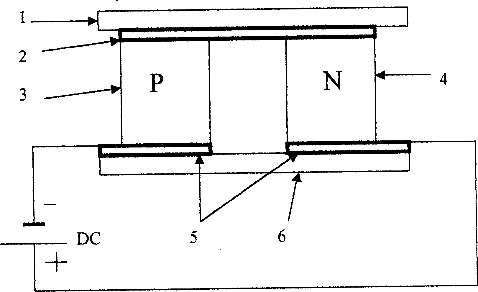
[0050] The basic unit of the thermoelectric semiconductor device of the present invention is a temperature difference thermocouple composed of a pair of P-type and N-type thermoelectric semiconductor elements, and the thermoelectric semiconductor elements are connected by metal strips. The finished thermoelectric semiconductor device is formed by connecting several pairs of thermoelectric semiconductor elements, and its composition is a series structure on the circuit, and a parallel structure in terms of heat conduction.

[0051] Figure 5 It is a structural schematic diagram of an upper base plate for installing a rectangular thermoelectric semiconductor element with a heat-conducting insulating substrate (1) equipped with a metal connecting piece (2);

[0052] Figure 6 It is a schematic diagram of the lower bottom plate structure and thermoelectric element installation of the rectangular thermoelectric semiconductor element installed with the thermally conductive insulati...

Embodiment approach 2

[0066] Such as Figure 8 Shown: the structure schematic diagram of the thermoelectric semiconductor device that the present invention proposes to be installed with another type of novel metal connecting piece (2b), (5b): among the figure (3) is a P-type thermoelectric semiconductor element, (4) N-type thermoelectric semiconductor element , (1), (6) are the upper and lower bottom plates respectively, (7b) is the partition (before casting is the casting model, after casting is the partition); after the metal connecting piece is bent, it penetrates into the P-type and N-type thermoelectric semiconductors element.

[0067] Others are the same as Embodiment 1, the thermoelectric semiconductor casting model is a disposable model: the specification of the model is consistent with the final product size of the thermoelectric semiconductor (supporting), and it is installed on the product to form a part of the product (before casting, it is a casting model, and after casting, it is a ther...

Embodiment approach 3

[0072] The thermoelectric semiconductor material melting furnace of the present invention adopts a specially designed melting furnace with constant temperature control, equipped with vacuum pumping and gas protection devices, and melts in a vacuum state, for example, heating and melting after vacuuming to 2Pa; transporting in a gas protection environment, such as using High-purity nitrogen or inert gas is used as a protective gas; the heating method of the melting furnace can use resistance heating methods: for example, heating by resistance heating elements such as resistance wires, electric heating tubes, and silicon carbide rods; induction eddy current heating methods can also be used: for example, frequency conversion Heating equipment uses electromagnetic waves to heat and melt raw materials. The working temperature range of the smelting furnace is controlled from 550°C to 850°C; the smelting process needs to be fully stirred to make the materials evenly combined. In this ...


PUM


Abstract

This invention discloses a method for manufacturing a thermal electric semiconductor device, the equipment and its products charactering in applying an accurate casting technology to directly cast the melt type P and type N thermal electric semiconductor materials to preset special models separately by quantitatively controlling the exit unit, which casts the materials onto the models separately by a conduit charactering that the P and N thermal electric elements are set at either side of a baffle, the bending part of the metal connection sheets is inserted into the elements and the plane part are fixed on the upper and the lower base plates.

Description

Technical field: [0001] The present invention relates to a method and equipment for manufacturing thermoelectric semiconductor devices and the products obtained therefrom. Background technique: [0002] Thermoelectric semiconductor devices are devices that use the Peltier effect generated when current passes through the P and N junctions of semiconductor materials to produce cooling or heating effects (according to the direction of the current). The structure and working principle schematic diagram of the typical thermoelectric semiconductor device of industrial production at present is as the accompanying drawing part of the description of the present invention figure 1 As shown, its basic unit is to connect a P-type thermoelectric semiconductor element (3) and an N-type thermoelectric semiconductor element (4) with metal connecting pieces (2), (5) to form a pair of thermocouples, and connect the DC power supply After (DC), there will be temperature difference and heat tra...

Claims


Application Information

Patent Timeline
Patent Type & Authority Applications(China)
IPC IPC(8): H01L35/34H01L35/28
Inventor 杜效中
Owner 杜效中
Why Eureka
Try Eureka