Cascading structure of semiconductor optical amplifiers for realizing full optical logic AND gate and/or NOT gate

A technology of optical amplifier and cascaded structure, which is applied in the direction of logic circuits using optoelectronic devices, logic circuits, and logic circuits using specific components, etc. It can solve the problems of four-wave mixing conversion efficiency limitation, impracticality, and difficulty in realization. Achieve the effect of improving the output signal quality, improving the output extinction ratio, and improving the stability

Inactive Publication Date: 2006-04-19
HUAZHONG UNIV OF SCI & TECH
View PDF0 Cites 13 Cited by
  • Summary
  • Abstract
  • Description
  • Claims
  • Application Information

AI Technical Summary

Problems solved by technology

The disadvantage of cross-phase modulation all-optical logic devices is that precise phase control is required, which is difficult to achieve with discrete components, and integrated devices must be used
The disadvantages of the all-optical logic device of the cross-polarization modulation type are: the input light is required to have the same power, the same polarization state, and the wavelength is similar, which is not practical; the p...

Method used


Image

  • Cascading structure of semiconductor optical amplifiers for realizing full optical logic AND gate and/or NOT gate
  • Cascading structure of semiconductor optical amplifiers for realizing full optical logic AND gate and/or NOT gate
  • Cascading structure of semiconductor optical amplifiers for realizing full optical logic AND gate and/or NOT gate

Examples


Embodiment Construction

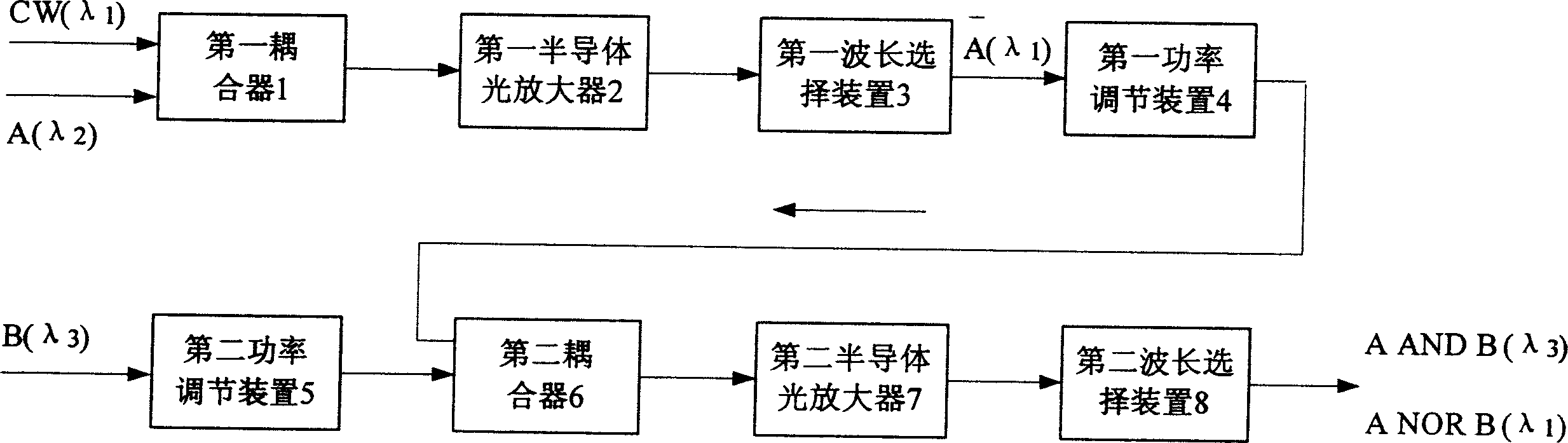
[0033] The invention uses the cascaded structure of semiconductor optical amplifiers to realize all-optical logic AND gates and NOR gates, and its theoretical basis is the cross-gain modulation effect of semiconductor optical amplifiers.

[0034] Depend on figure 2 As shown, the CW light and the signal light A are respectively connected to the input end of the first coupler 1, and the output end of the first coupler 1 is sequentially connected to the first semiconductor optical amplifier 2, the first wavelength selection device 3, the first power regulator device 4; the signal light B is connected to the input end of the second power adjustment device 5, the output ends of the first power adjustment device 4 and the second power adjustment device 5 are respectively connected to the input end of the second coupler 6, and the second coupling The output terminal of the device 6 is connected to the second semiconductor optical amplifier 7 and the second wavelength selection devic...


PUM


Abstract

The cascading structure is as following: CW light and signal light A are connected to the input end of the first coupler respectively; the output of the first coupler is connected to the first optical amplifier of semiconductor, first wavelength selector, and first power regulating device; signal light B is connected to the input end of the second coupler; output end of first power regulating device and output end of second power regulating device are connected to the input end of the second coupler; the output end of the second coupler is connected to second optical amplifier of semiconductor, second wavelength selector in sequence; through adjusting output powers of first power regulating device and second power regulating device can obtain full optical logic AND gate and/or NOT gate at different output wavelengths of the second wavelength selector. The invention realizes advantages of full optical logic device in crossed gain modulation type, and based on same class of structure.

Description

technical field [0001] The invention relates to a semiconductor optical amplifier (SOA) cascade structure, in particular to a semiconductor optical amplifier cascade structure for realizing all-optical logic gates. Background technique [0002] In recent years, the service range of IP business has developed from the initial simple E-mail to business and multimedia services. Various new services, such as videophone, high-definition television (HDTV), telemedicine, home office, etc., are booming. However, in the existing communication network based on electronic technology, each node of the network needs to complete the optical / electrical / optical conversion, and the electronic devices in it are limited by the upper limit rate of 40G. In terms of meeting the needs of high speed and large capacity, there are Such disadvantages as bandwidth limitation, clock skew, severe crosstalk, high power consumption, etc. have resulted in the phenomenon of "electronic bottleneck" in the com...

Claims


Application Information

Patent Timeline
IPC IPC(8): G02F3/00
Inventor 张新亮赵婵黄德修董建绩刘德明
Owner HUAZHONG UNIV OF SCI & TECH
Why Eureka
Try Eureka